

ST 74V1T05 User Manual
查询74V1T05供应商
SINGLE INVERTER(OPEN DRAIN)
■ HIGHSPEED:t
■ LOW POWER DISSIPATION:
=1 µA (MAX.)at TA=25oC
I
CC
■ COMPATIBLEWITHTTLOUTPUTS:
=2V(MIN),VIL=0.8V(MAX)
V
IH
■ POWERDOWNPROTECTIONON INPUTS
■ OPERATINGVOLTAGERANGE:
(OPR)= 4.5Vto 5.5V
V
CC
■ IMPROVEDLATCH-UPIMMUNITY
DESCRIPTION
The 74V1T05 is an advanced high-speed CMOS
SINGLE INVERTER (OPEN DRAIN) fabricated
with sub-micron silicon gate and double-layer
metalwiring C
The internal circuit is composed of 3 stages
including buffer output, which provide high noise
immunityand stableoutput.
=6ns (TYP.)atVCC=5V
PD
2
MOStechnology.
74V1T05
PRELIMINARY DATA
S
(SOT23-5L)
ORDERCODE:
74V1T05S 74V1T05C
This device can, with an external pull-up resistor,
be used in wired AND configuration. This device
can also be used as a led driver in any other
applicationrequiring a currentsink.
Power down protection is provided on inputand 0
to 7V can be accepted on inputwith no regard to
the supply voltage. This device can be used to
interface5V to 3V.
C
(SC-70)
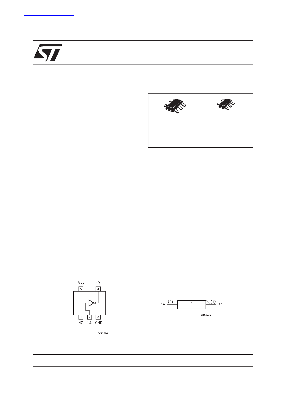
PIN CONNECTION AND IEC LOGICSYMBOLS
September 1999
1/7
74V1T05
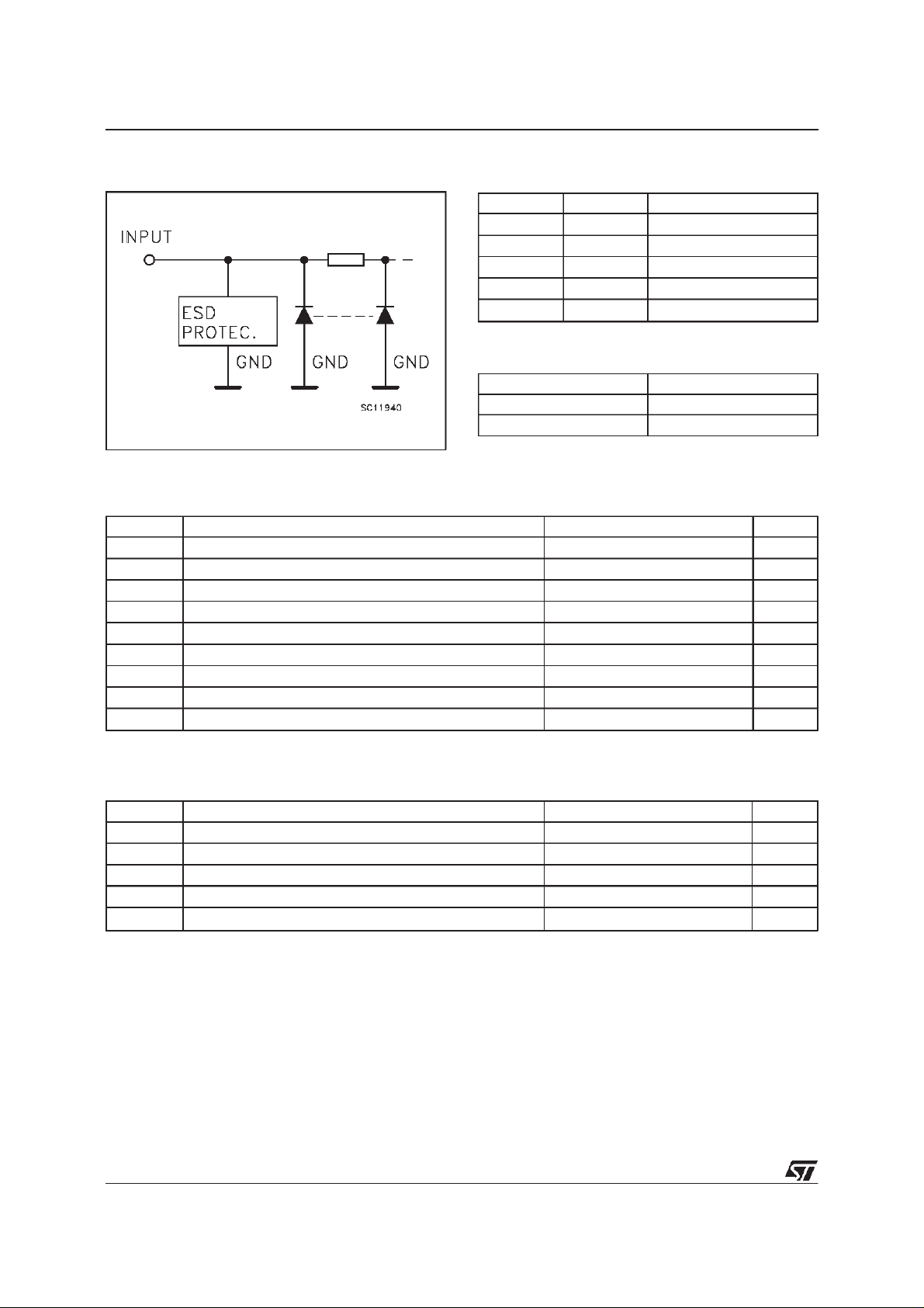
INPUT EQUIVALENTCIRCUIT
PIN DESCRIPTION
PI N No SYMB OL NAME AND F U NCTIO N
1 N.C. Not Connected
2 1A Data Input
4 1Y Data Output
3 GND Ground (0V)
5V
CC
Positive Supply Voltage
TRUTH TABLE
AY
LZ
HL
Z: High Impedance
ABSOLUTE MAXIMUM RATINGS
Symb o l Para met er Val u e Uni t
V
V
V
I
I
OK
I
or I
I
CC
T
T
AbsoluteMaximumRatingsarethosevaluesbeyondwhichdamageto thedevicemayoccur.Functionaloperationunderthesecondition isnotimplied.
Supply Voltage -0.5 to +7.0 V
CC
DC Input Voltage -0.5 to +7.0 V
I
DC Output Voltage -0.5 to VCC+ 0.5 V
O
DC Input Diode Current - 20 mA
IK
DC Output Diode Current
DC Output Current 25 mA
O
DC VCCor Ground Current ± 50 mA
GND
Storage Temperature -65 to +150
stg
Lead Temperature (10 sec) 260
L
20 mA
±
o
C
o
C
RECOMMENDED OPERATINGCONDITIONS
Symb o l Para met er Value Un it
V
V
V
T
dt/dv
1) VINfrom0.8Vto2 V
2/7
Supply Voltage 4.5 to 5.5 V
CC
Input Voltage 0 to 5.5 V
I
Output Voltage 0 to V
O
Operating Temperature -40 to +85
op
Input Rise and Fall Time (see note 1) (V
=5.0±0.5V)
CC
CC
0 to 20 ns/V
V
o
C
74V1T05
DC SPECIFICATIONS
Symb o l Para met er Test Con diti o ns Val u e Uni t
T
V
CC
High Level Input
V
IH
(V)
4.5 to 5.5 2 2 V
Min. Typ. Max. Min. Max.
Voltage
V
IL
Low Level Input
4.5 to 5.5 0.8 0.8 V
Voltage
Low Level Output
V
OL
Voltage
High Impedance
I
OZ
Output Leakage
4.5 IO=50 µ A 0.0 0.1 0.1
4.5 I
5.5
=8 mA 0.36 0.44
O
VI=VIHor V
IL
VO=VCCor GND
Current
Input Leakage Current 0 to 5.5 VI= 5.5V or GND
I
I
Quiescent Supply
I
CC
5.5 VI=VCCorGND 1 10 µA
Current
Additional Worst Case
I
∆
CC
Supply Current
5.5 One Input at 3.4V,
other input at V
CC
or
GND
=25oC -40 to 85oC
A
0.25
±
0.1
±
1.35 1.5 mA
2.5
±
1.0
±
µ
µ
V
A
A
AC ELECTRICAL CHARACTERISTICS
(Inputt
r=tf
=3 ns)
Symbol Parameter Test Condition Value Unit
V
(*)
t
Propagation Delay
PLz
t
Time
PzL
(*)Voltagerange is5V ± 0.5V
CC
(V)
C
(pF)
L
5.0 15 RL=1K
5.0
50 R
=1KΩ 6.5 8.0 1.0 9.0
L
Min. Typ. Max. Min. Max.
Ω
=25oC -40 to 85oC
T
A
6.0 7.0 1.0 8.0
ns
CAPACITIVE CHARACTERISTICS
Symb o l Para met er Test Con diti o ns Val u e Uni t
=25oC -40 to 85oC
T
A
Min. Typ. Max. Min. Max.
C
Input Capacitance 4 10 10
IN
C
Output Capacitance 5
OUT
Power Dissipation
C
PD
10.5 pF
Capacitance (note 1)
1)CPDisdefined asthevalue oftheIC’sinternal equivalentcapacitance whichiscalculated fromtheoperating currentconsumption without load.(Referto
TestCircuit).Average operatingcurrent canbeobtainedbythefollowingequation.I
(opr)= CPD• VCC• fIN+I
CC
CC
pF
pF
3/7
 Loading...