

ST 74V1GU04 User Manual
74V1GU04
SINGLE INVERTER (SINGLE STAGE)
■ HIGH SPEED: t
■ LOW POWER DISSIPATION:
I
=1µA(MAX.) at TA=25°C
CC
■ HIGH NOISE IMMUNITY:
V
NIH=VNIL
■ POWER DOWN PROTECTION ON INPUT
■ SYMMETRICAL OUTPUTIMPEDANCE:
|I
|=IOL=8mA(MIN)atVCC=4.5V
OH
■ BALANCED PROPAGATION DELAYS:
t
≅ t
PLH
■ OPERATING VOLTAGE RANGE:
V
(OPR) = 2V to 5.5V
CC
■ IMPROVED LATCH-UP IMMUNITY
= 10% VCC(MIN.)
PHL
= 3.5ns (TYP.) at VCC=5V
PD
DESCRIPTION
The 74V1GU04 is an advanced high-speed
CMOS SINGLE INVERTER (SINGLE STAGE)
fabricated with sub-micron silicon gat e and
double-layer metal wiring C
2
MOS technology.
The internal circuit is composed of a single stages
inverter, then an unbuffered output.
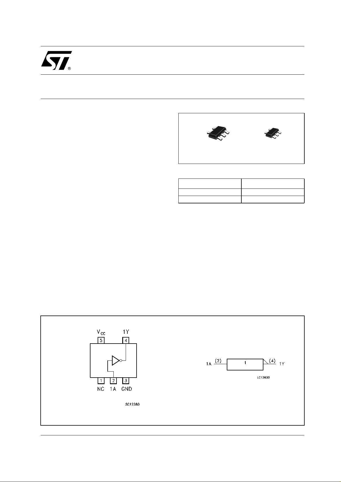
SOT323-5LSOT23-5L
ORDER CODES
PACKAGE T & R
SOT23-5L 74V1GU04STR
SOT323-5L 74V1GU04CTR
it can be used in analog applicat ion such a crystal
oscillator.
Power down protection is provided on inpu t and 0
to 7V c an be acce pted on input with no regard to
the supply voltage. This device can be used to
interface5Vto3V.
PIN CONNECTION AND IEC LOGIC SYMBOLS
1/9April 2004
74V1GU04
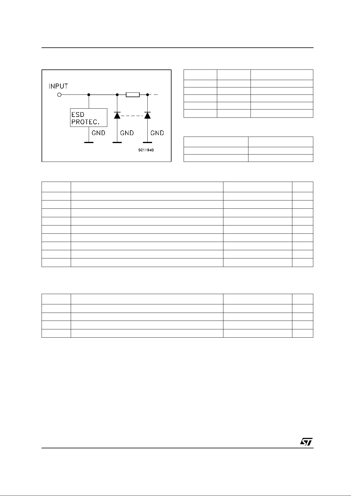
INPUT EQUIVALENT CIRCUIT PIN DESCRIPTION
PIN N° SYMBOL NAME AND FUNCTION
1 NC Not Connected
2 1A Data Input
4 1Y Data Output
3 GND Ground (0V)
5
TRUTH TABLE
ABSOLUTE MAXIMUM RATINGS
Symbol Parameter Value Unit
V
V
V
I
I
OK
I
I
or I
CC
T
T
Absolute Maximum Ratings are those values beyond which damage to the device may occur. Functional operation under these conditions is
not implied.
Supply Voltage
CC
DC Input Voltage
I
DC Output Voltage -0.5 to VCC+0.5
O
DC Input Diode Current
IK
DC Output Diode Current
DC Output Current
O
DC VCCor Ground Current
GND
Storage Temperature
stg
Lead Temperature (10 sec)
L
V
CC
Positive Supply Voltage
AY
LH
HL
-0.5 to +7.0 V
-0.5 to +7.0 V
V
-20 mA
± 20 mA
± 25 mA
± 50 mA
-65 to +150 °C
260 °C
RECOMMENDED OPERATING CONDITIONS
Symbol Parameter Value Unit
V
V
V
T
2/9
Supply Voltage
CC
Input Voltage
I
Output Voltage 0 to V
O
Operating Temperature
op
2to5.5 V
0to5.5 V
CC
-55 to 125 °C
V
DC SPECIFICATIONS
Symbol Parameter
V
V
V
High Level Input
IH
Voltage
V
Low Level Input
IL
Voltage
High Level Output
OH
Voltage
Low Level Output
OL
Voltage
Input Leakage
I
I
Current
I
Quiescent Supply
CC
Current
74V1GU04
Test Condition Value
T
= 25°C
V
CC
(V)
A
Min. Typ. Max. Min. Max. Min. Max.
2.0 1.7 1.7 1.7
3.0to
5.5
0.8V
CC
2.0 0.3 0.3 0.3
3.0to
5.5
2.0
3.0
4.5
3.0
4.5
2.0
3.0
4.5
3.0
4.5
0to
5.5
5.5
IO=-50 µA
=-50 µA
I
O
=-50 µA
I
O
=-4 mA
I
O
I
=-8 mA
O
IO=50 µA
I
=50 µA
O
=50 µA
I
O
=4 mA
I
O
I
=8 mA
O
VI=5.5VorGND
V
I=VCC
or GND
1.8 2.0 1.8 1.8
2.7 3.0 2.7 2.7
4.0 4.5 4.0 4.0
2.58 2.48 2.4
3.94 3.8 3.7
0.2V
0.0 0.2 0.2 0.2
0.0 0.3 0.3 0.3
0.0 0.5 0.5 0.5
-40 to 85°C -55 to 125°C
CC
0.8V
CC
0.2V
CC
0.8V
CC
0.36 0.44 0.55
0.36 0.44 0.55
± 0.1 ± 1 ± 1 µA
11020µA
0.2V
CC
Unit
V
V
V
V
AC ELECTRICAL CHARACTERISTICS (Input t
r=tf
=3ns)
Test Condition Value
= 25°C
Symbol Parameter
t
PLHtPHL
(*) Voltage rangeis 3.3V ± 0.3V
(**) Voltage range is 5.0V ± 0.5V
Propagation Delay
Time
V
3.3
3.3
5.0
5.0
C
CC
(V)
L
(pF)
(*)
15 4.4 6.5 1.0 8.0 1.0 9.0
(*)
50 4.8 7.0 1.0 9.0 1.0 10.0
(**)
15 3.5 5.5 1.0 6.0 1.0 7.5
(**)
50 4.1 6.0 1.0 7.0 1.0 8.0
T
A
-40 to 85°C -55 to 125°C
Min. Typ. Max. Min. Max. Min. Max.
Unit
ns
CAPACITIVE CHARACTERISTICS
Test Condition Value
T
Symbol Parameter
C
C
Input Capacitance
IN
Power Dissipation
PD
Capacitance
(note 1)
1) CPDis defined as the value of the IC’s internal equivalent capacitance which is calculated from the operating current consumption without
load. (Refer to Test Circuit). Average operating current can be obtained by the following equation. I
= 25°C
A
-40 to 85°C -55 to 125°C
Min. Typ. Max. Min. Max. Min. Max.
510 10 10pF
10 pF
CC(opr)=CPDxVCCxfIN+ICC
Unit
3/9
 Loading...