


Features
■ High speed:
t
= 0.3 ns (typ.) at VCC = 5 V
PD
t
= 0.4 ns (typ.) at VCC = 3.3 V
PD
■ Low power dissipation:
I
= 1 μA (max.) at TA=25°C
CC
■ Low "ON" resistance:
R
=6.5Ω (typ.) at VCC = 5 V I
ON
R
= 8.5 Ω (typ.) at VCC = 3.3 V I
ON
■ Sine wave distortion:
0.04% at V
■ Wide operating range:
V
(opr) = 2 V to 5.5 V
CC
■ Improved latch-up immunity
= 3.3V f = 1kHz
CC
= 1 mA
I/O
= 1 mA
I/O
74V1G66
Single bilateral switch
SOT23-5L
SOT323-5L
Description
The 74V1G66 is an advanced high-speed CMOS
single bilateral switch fabricated in silicon gate
2
C
MOS technology. It achieves high speed
propagation delay and very low ON resistances
while maintaining true CMOS low power
consumption. This bilateral switch handles rail to
rail analog and digital signals that may vary
across the full power supply range (from GND to
V
).
CC
The C input is provided to control the switch and it
is compatible with standard CMOS outputs. The
switch is ON (port I/O is connected to port O/I)
when the C input is held high and OFF (high
impedance state exists between the two ports)
when C is held low. It can be used in many
applications as battery powered systems or test
equipments.
Table 1. Device summary
Order code Package Packaging
74V1G66STR SOT23-5L Tape and reel
The 74V1G66 is available in the commercial and
extended temperature range in SOT23-5L and
SOT323-5L packages.
All inputs and outputs are equipped with
protection circuits against static discharge, giving
them ESD immunity and transient excess voltage.
74V1G66CTR SOT323-5L Tape and reel
October 2008 Rev 8 1/15
www.st.com
15

Pin connection 74V1G66
1 Pin connection
Figure 1. Pin connection and IEC logic symbols
6##
#
)/ /) '.$
Table 2. Pin description
Pin number Symbol Name and function
1 I/O Independent input/output
2 O/I Independent output/input
3 GND Ground (0 V)
4 C Enable input (active high)
5V
CC
)/
#
8)
)
)
/)
!-6
Positive supply voltage
Figure 2. Input equivalent circuit
)/
#
).
Table 3. Truth table
Control Switch function
HON
LOFF
1. High impedance state.
/)
!-6
(1)
2/15

74V1G66 Maximum rating
2 Maximum rating
Stressing the device above the rating listed in the “Absolute Maximum Ratings” table may
cause permanent damage to the device. These are stress ratings only and operation of the
device at these or any other conditions above those indicated in the Operating sections of
this specification is not implied. Exposure to Absolute Maximum Rating conditions for
extended periods may affect device reliability.
Table 4. Absolute maximum ratings
Symbol Parameter Value Unit
I
CC
I
V
V
V
I
GND
T
Supply voltage -0.5 to +7.0 V
CC
DC input voltage -0.5 to VCC + 0.5 V
V
I
DC control input voltage -0.5 to +7.0 V
IC
DC Output voltage -0.5 to VCC + 0.5 V
O
DC input diode current ± 20 mA
I
IK
I
DC control input diode current - 20 mA
IK
DC output diode current ± 20 mA
OK
DC output current ± 50 mA
I
O
or
DC VCC or ground current ± 50 mA
Storage temperature -65 to +150 °C
stg
T
Lead temperature (10 sec) 300 °C
L
Table 5. Recommended operating conditions
Symbol Parameter Value Unit
V
V
V
T
dt/dv Input rise and fall time
1. VIN from 30% to 70% of VCC on control pin.
Supply voltage 2 to 5.5 V
CC
Input voltage 0 to V
V
I
Control input voltage 0 to 5.5 V
IC
Output voltage 0 to V
O
Operating temperature -55 to 125 °C
op
(1)
VCC = 5.0 V
0 to 20 ns/V
CC
CC
V
V
3/15

Maximum rating 74V1G66
Table 6. DC specifications
Test condition Value
Symbol Parameter
V
V
R
R
High level input
IH
voltage
Low level input
IL
voltage
ON resistance
ON
ON resistance
ON
Input/output
I
OFF
leakage current
(switch OFF)
Switch input
leakage current
I
IZ
(switch ON, output
open)
V
CC
TA = 25°C -40 to 85°C
-55 to
125°C
(V)
Min Typ Max Min Max Min Max
2.0 1.5 1.5 1.5
2.7 to
5.5
0.7V
C
C
0.7V
CC
0.7V
CC
2.0 0.5 0.5 0.5
2.7 to
5.5
(1)
3.3
(2)
5.0
(1)
3.3
(2)
5.0
VIC = VIH
V
= VCC to
I/O
GND
≤ 1mA
I
I/O
VIC = VIH
= VCC or
V
I/O
GND
I
≤ 1mA
I/O
0.3V
C
C
0.3V
CC
12.5 21 23 27
7.5 10 12 14
8.5 11.5 12.5 15
6.5 8.5 10 12
VOS = VCC to
GND
5.5
VIS = VCC to
±0.1 ± 1 ± 5 μA
GND
= V
V
IC
IL
= VCC to
V
OS
5.5
V
GND
= V
IC
IH
±0.1 ± 1 ± 5 μA
0.3V
CC
Unit
V
V
Ω
Ω
Control input
I
IN
leakage current
I
1. Voltage range is 3.3 V ± 0.3 V.
2. Voltage range is 5 V ± 0.5 V.
Quiescent supply
CC
current
0 to
5.5
5.5
VIC = 5.5V or
GND
= VCC or
V
I
GND
4/15
± 0.1 ± 1.0 ± 1.0 μA
11020μA

74V1G66 Maximum rating
Table 7. AC electrical characteristics (CL = 50 pF, input tr = tf = 3 ns)
Test condition Value
Symbol Parameter
= 25°C -40 to 85°C
T
V
CC
A
-55 to
125°C
(V)
Min Typ Max Min Max Min Max
(1)
t
t
t
PHZ
t
t
PZH
1. Voltage range is 3.3 V ± 0.3 V.
2. Voltage range is 5 V ± 0.5 V.
Delay time
PD
Output disable
PLZ
time
PZL
Output enable time
3.3
5.0
3.3
5.0
3.3
5.0
(2)
(1)
(2)
(1)
(2)
tr = tf = 6 ns
RL = 500 Ω
RL = 1 KΩ
0.4 0.8 1.2 2.4
0.3 0.6 1.0 2.0
5.0 7.5 9.0 10.0
5.0 7.5 9.0 10.0
2.5 4.0 5.0 7.0
2.0 4.0 5.0 7.0
Table 8. Capacitive characteristics
Test condition Value
Symbol Parameter
V
CC
TA = 25°C -40 to 85°C
(V)
Min Typ Max Min Max Min Max
C
C
C
1. CPD is defined as the value of the IC’s internal equivalent capacitance which is calculated from the operating current
consumption without load. (Refer to the test circuit). Average operating current can be obtained by the following equation.
I
Input capacitance 3 10 10 10 pF
IN
Output
I/O
capacitance
Power dissipation
PD
capacitance
(opr) = CPD x VCC x fIN + ICC.
CC
(1)
3.3 2.5
5.0 3
10 pF
-55 to
125°C
Unit
ns
ns
ns
Unit
pF
5/15

Maximum rating 74V1G66
Table 9. Analog switch characteristics (GND = 0 V; TA = 25°C)
Symbol Parameter
Sine wave
distortion (THD)
Frequency
f
MAX
response
(switch ON)
Feed through
attenuation
(switch OFF)
Crosstalk
(control input to
signal output)
1. Voltage range is 3.3 V ± 0.3 V
2. Voltage range is 5.0 V ±
0.5 V
Test condition
V
V
(V)
3.3
5.0
3.3
5.0
3.3
5.0
3.3
5.0
IN
CC
(V
p-
)
p
(1)
2.75
(2)
40.04
(1)
Adjust fIN voltage to obtain 0 dBm at VOS.
Increase fIN Frequency until dB meter reads -3dB
(2)
RL = 50 Ω, CL = 10 pF
(1)
V
is centered at VCC/2
IN
Adjust fIN Voltage to obtained 0dBm at VIS
(2)
RL = 600Ω, CL = 50 pF, fIN = 1KHz sine wave
(1)
= 1 KHz RL = 10 KΩ, CL = 50 pF
f
IN
RL = 600 Ω, CL = 50 pF, fIN = 1 KHz square wave
(2)
= tf = 6 ns
t
r
Val u
e
Unit
Typ
0.04
%
150
MHz
180
-60
dB
-60
60
mV
60
6/15

74V1G66 Switching characteristics test circuit
3 Switching characteristics test circuit
Figure 3. Enable and disable timing (circuit) Figure 4. Enable and disable timing
(waveform)
Figure 5. Resistive feedthrough attenuation Figure 6. Capacitive feedthrough attenuation
AM00744V1
Figure 7. Bandwidth attenuation Figure 8. Maximum control frequency
7/15

Switching characteristics test circuit 74V1G66
Figure 9. Crosstalk (control to output)
Figure 10. Channel resistance (R
Figure 11. I
CC
(opr)
ON
)
8/15

74V1G66 Package mechanical data
4 Package mechanical data
In order to meet environmental requirements, ST offers these devices in ECOPACK®
packages. These packages have a Lead-free second level interconnect. The category of
second level interconnect is marked on the package and on the inner box label, in
compliance with JEDEC Standard JESD97. The maximum ratings related to soldering
conditions are also marked on the inner box label. ECOPACK is an ST trademark.
ECOPACK specifications are available at: www.st.com.
9/15

Package mechanical data 74V1G66
SOT23-5L MECHANICAL DATA
DIM.
MIN. TYP MAX. MIN. TYP. MAX.
A 0.90 1.45 35.4 57.1
A1 0.00 0.10 0.0 3.9
A2 0.90 1.30 35.4 51.2
b 0.35 0.50 13.7 19.7
C 0.09 0.20 3.5 7.8
D2.80 3 .00 110.2 118.1
E 1.50 1.75 59.0 68.8
e0.95 37.4
H 2.60 3 .00 102.3 118.1
L 0.10 0.60 3.9 23.6
mm. mils
.
10/15
7049676C

74V1G66 Package mechanical data
SOT323-5L MECHANICAL DATA
DIM.
A0.80 1.10 31.5 43.3
A1 0.00 0.10 0.0 3.9
A2
b 0.15 0.30 5.9 11.8
C 0.10 0.183.9 7.1
D1.80 2.20 70.9 86.6
E1.80 2.40 70.9 94.5
E1 1.15 1.35 45.3 53.1
e
e1
L 0.10 0.30 3.9 11.8
MIN. TYP MAX.
0.80 1.00 31.5 39.4
mm. mils
MIN. TYP. MAX.
.65
0
1.3 51.2
25.6
11/15

Package mechanical data 74V1G66
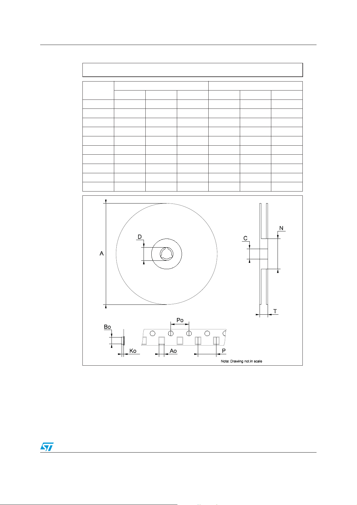
Tape & Reel SOT23-xL MECHANICAL DATA
DIM.
A1807.086
C 12.8 13.0 13.2 0.504 0.512 0.519
D 20.2 0.795
N60 2.362
T 14.4 0.567
Ao 3.133.233.33 0.123 0.127 0.131
Bo 3.07 3.17 3.27 0.120 0.124 0.128
Ko
Po 3.9 4.0 4.1 0.153 0.157 0.161
P 3.9 4.0 4.1 0.153 0.157
MIN. TYP MAX. MIN. TYP. MAX.
1.27 1.37 1.47 0.050 0.054 0.058
mm. inch
0.161
12/15
74V1G66 Package mechanical data
Tape & Reel SOT323-xL MECHANICAL DATA
DIM.
A 175 1801856.8897.0867.283
C 12.8 13 13.2 0.504 0.512 0.519
D 20.2 0.795
N 59.5 60 60.5 2.362
T 14.4 0.567
Ao 2.25 0.088
Bo 2.7 0.106
Ko
Po 3.9 4 4.1 0.153 0.157 0.161
P 3.8 4 4.2 0.149 0.157
MIN. TYP MAX. MIN. TYP. MAX.
mm. inch
1.2 0.047
0.165
13/15

Revision history 74V1G66
5 Revision history
Table 10. Document revision history
Date Revision Changes
01-Apr-2004 7 Updated data reel information.
28-Oct-2008 8
Document reformatted to improve readability.
Updated Table 6: DC specifications on page 4.
14/15

74V1G66
Please Read Carefully:
Information in this document is provided solely in connection with ST products. STMicroelectronics NV and its subsidiaries (“ST”) reserve the
right to make changes, corrections, modifications or improvements, to this document, and the products and services described herein at any
time, without notice.
All ST products are sold pursuant to ST’s terms and conditions of sale.
Purchasers are solely responsible for the choice, selection and use of the ST products and services described herein, and ST assumes no
liability whatsoever relating to the choice, selection or use of the ST products and services described herein.
No license, express or implied, by estoppel or otherwise, to any intellectual property rights is granted under this document. If any part of this
document refers to any third party products or services it shall not be deemed a license grant by ST for the use of such third party products
or services, or any intellectual property contained therein or considered as a warranty covering the use in any manner whatsoever of such
third party products or services or any intellectual property contained therein.
UNLESS OTHERWISE SET FORTH IN ST’S TERMS AND CONDITIONS OF SALE ST DISCLAIMS ANY EXPRESS OR IMPLIED
WARRANTY WITH RESPECT TO THE USE AND/OR SALE OF ST PRODUCTS INCLUDING WITHOUT LIMITATION IMPLIED
WARRANTIES OF MERCHANTABILITY, FITNESS FOR A PARTICULAR PURPOSE (AND THEIR EQUIVALENTS UNDER THE LAWS
OF ANY JURISDICTION), OR INFRINGEMENT OF ANY PATENT, COPYRIGHT OR OTHER INTELLECTUAL PROPERTY RIGHT.
UNLESS EXPRESSLY APPROVED IN WRITING BY AN AUTHORIZED ST REPRESENTATIVE, ST PRODUCTS ARE NOT
RECOMMENDED, AUTHORIZED OR WARRANTED FOR USE IN MILITARY, AIR CRAFT, SPACE, LIFE SAVING, OR LIFE SUSTAINING
APPLICATIONS, NOR IN PRODUCTS OR SYSTEMS WHERE FAILURE OR MALFUNCTION MAY RESULT IN PERSONAL INJURY,
DEATH, OR SEVERE PROPERTY OR ENVIRONMENTAL DAMAGE. ST PRODUCTS WHICH ARE NOT SPECIFIED AS "AUTOMOTIVE
GRADE" MAY ONLY BE USED IN AUTOMOTIVE APPLICATIONS AT USER’S OWN RISK.
Resale of ST products with provisions different from the statements and/or technical features set forth in this document shall immediately void
any warranty granted by ST for the ST product or service described herein and shall not create or extend in any manner whatsoever, any
liability of ST.
ST and the ST logo are trademarks or registered trademarks of ST in various countries.
Information in this document supersedes and replaces all information previously supplied.
The ST logo is a registered trademark of STMicroelectronics. All other names are the property of their respective owners.
© 2008 STMicroelectronics - All rights reserved
STMicroelectronics group of companies
Australia - Belgium - Brazil - Canada - China - Czech Republic - Finland - France - Germany - Hong Kong - India - Israel - Italy - Japan -
Malaysia - Malta - Morocco - Singapore - Spain - Sweden - Switzerland - United Kingdom - United States of America
www.st.com
15/15
 Loading...