

ST 74V1G14 User Manual
74V1G14C
74V1G14
SINGLE SCHMITT INVERTER
■HIGH SPEED: tPD = 5.5 ns (TYP.) at VCC = 5V
■LOW POWER DISSIPATION: ICC = 1 μA (MAX.) at TA = 25 oC
■TYPICAL HYSTERESIS: Vh = 1V AT VCC=4.5V
■POWER DOWN PROTECTION ON INPUTS
■SYMMETRICAL OUTPUT IMPEDANCE: |IOH| = IOL = 8 mA (MIN)
■BALANCED PROPAGATION DELAYS:
tPLH tPHL
■OPERATING VOLTAGE RANGE: VCC (OPR) = 2V to 5.5V
■IMPROVED LATCH-UP IMMUNITY
DESCRIPTION
The 74V1G14 is an advanced high-speed CMOS SINGLE SCHMITT INVERTER fabricated with sub-micron silicon gate and double-layer metal wiring C2MOS technology.
The internal circuit is composed of 3 stages including buffer output, which provide high noise immunity and stable output.
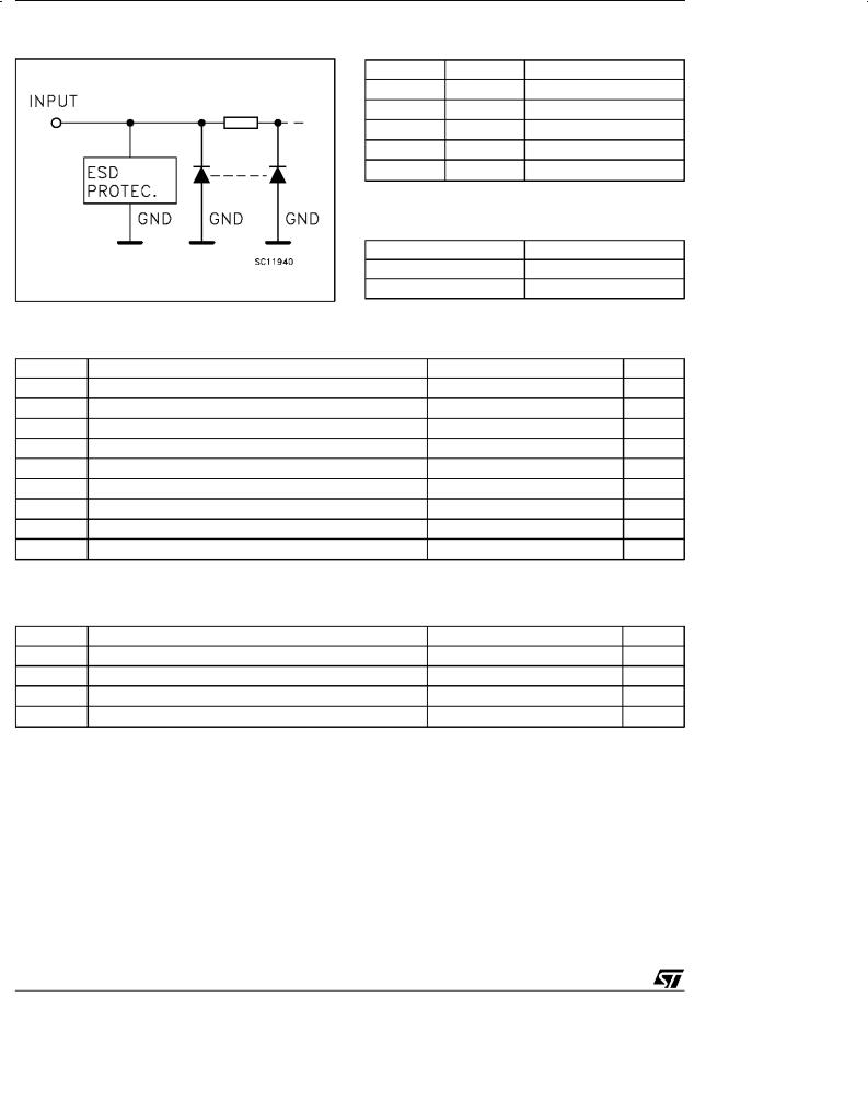
Power down protection is provided on all inputs and 0 to 7V can be accepted on inputs with no
PIN CONNECTION AND IEC LOGIC SYMBOLS
S |
C |
(SOT23-5L) |
(SC-70) |
ORDER CODE:
74V1G14S 74V1G14C
regard to the supply voltage. This device can be used to interface 5V to 3V.
Pin configuration and function are the same as those of the V1G04 but the V1G14 has hysteresis.
This together with its schmitt trigger function allows it to be used on line receivers with slow rise/fall input signals.
All inputs and outputs are equipped with protection circuits against static discharge, giving them 2KV ESD immunity and transient excess voltage.
October 1999 |
1/7 |
74V1G14
INPUT EQUIVALENT CIRCUIT |
PIN DESCRIPTION |
|
|
|
PI N No |
SYMBOL |
NAME AND FUNCT ION |
|
1 |
N.C. |
Not Connected |
|
2 |
1A |
Data Input |
|
4 |
1Y |
Data Output |
|
3 |
GND |
Ground (0V) |
|
5 |
VCC |
Positive Supply Voltage |
|
TRUTH TABLE |
|
|
|
A |
|
Y |
|
L |
|
H |
|
H |
|
L |
ABSOLUTE MAXIMUM RATINGS |
|
|
|
Symbol |
Parameter |
Val ue |
Unit |
VCC |
Supply Voltage |
-0.5 to +7.0 |
V |
VI |
DC Input Voltage |
-0.5 to +7.0 |
V |
VO |
DC Output Voltage |
-0.5 to VCC + 0.5 |
V |
IIK |
DC Input Diode Current |
- 20 |
mA |
IOK |
DC Output Diode Current |
± 20 |
mA |
IO |
DC Output Current |
± 25 |
mA |
ICC or IGND |
DC VCC or Ground Current |
± 50 |
mA |
Tstg |
Storage Temperature |
-65 to +150 |
oC |
TL |
Lead Temperature (10 sec) |
260 |
oC |
Absolute Maximum Ratings are those values beyond which damage to the device may occur. Functional operation under these condition is not implied.
RECOMMENDED OPERATING CONDITIONS
Symbol |
Parameter |
Valu e |
Uni t |
VCC |
Supply Voltage |
2.0 to 5.5 |
V |
VI |
Input Voltage |
0 to 5.5 |
V |
VO |
Output Voltage |
0 to VCC |
V |
Top |
Operating Temperature |
-40 to +85 |
oC |
2/7

|
|
|
|
|
|
|
|
74V1G14 |
|
DC SPECIFICATIONS |
|
|
|
|
|
|
|
|
|
Symb ol |
Parameter |
T est Cond ition s |
|
|
Val ue |
|
|
Un it |
|
|
|
VCC |
|
TA = 25 oC |
-40 to 85 oC |
|
|||
|
|
(V) |
|
Min. Typ . Max. Min . Max. |
|
||||
|
|
|
|
|
|||||
Vt+ |
High Level Input |
3.0 |
|
2.2 |
|
|
2.2 |
|
|
|
Voltage |
4.5 |
|
3.15 |
|
|
3.15 |
|
V |
|
|
|
|
|
|
|
|||
|
|
5.5 |
|
3.85 |
|
|
3.85 |
|
|
Vt- |
Low Level Input |
3.0 |
|
|
|
0.9 |
|
0.9 |
|
|
Voltage |
4.5 |
|
|
|
1.35 |
|
1.35 |
V |
|
|
5.5 |
|
|
|
1.65 |
|
1.65 |
|
Vh |
Hysteresis Voltage |
3.0 |
|
0.3 |
|
1.2 |
0.3 |
1.2 |
|
|
|
4.5 |
|
0.4 |
|
1.4 |
0.4 |
1.4 |
V |
|
|
|
|
|
|||||
|
|
5.5 |
|
0.5 |
|
1.6 |
0.5 |
1.6 |
|
VOH |
High Level Output |
2.0 |
IO=-50 μA |
1.9 |
2.0 |
|
1.9 |
|
|
|
Voltage |
3.0 |
IO=-50 μA |
2.9 |
3.0 |
|
2.9 |
|
V |
|
|
4.5 |
IO=-50 μA |
4.4 |
4.5 |
|
4.4 |
|
|
|
|
|
|
|
|||||
|
|
3.0 |
IO=-4 mA |
2.58 |
|
|
2.48 |
|
|
|
|
4.5 |
IO=-8 mA |
3.94 |
|
|
3.8 |
|
|
VOL |
Low Level Output |
2.0 |
IO=50 μA |
|
0.0 |
0.1 |
|
0.1 |
|
|
Voltage |
3.0 |
IO=50 μA |
|
0.0 |
0.1 |
|
0.1 |
V |
|
|
4.5 |
IO=50 μA |
|
0.0 |
0.1 |
|
0.1 |
|
|
|
|
|
|
|||||
|
|
3.0 |
IO=4 mA |
|
|
0.36 |
|
0.44 |
|
|
|
4.5 |
IO=8 mA |
|
|
0.36 |
|
0.44 |
|
II |
Input Leakage Current |
0 to 5.5 |
VI = 5.5V or GND |
|
|
±0.1 |
|
±1.0 |
μA |
ICC |
Quiescent Supply |
5.5 |
VI = VCC or GND |
|
|
1 |
|
10 |
μA |
|
Current |
|
|
|
|
|
|
|
|
AC ELECTRICAL CHARACTERISTICS (Input tr = tf =3 ns) |
|
|
|
|
|
|
|||
Symb ol |
Parameter |
Test Co nditi on |
|
|
Val ue |
|
|
Un it |
|
|
|
VCC |
CL |
TA = 25 oC |
-40 to 85 oC |
|
|||
|
|
(V) |
(pF ) |
Min. Typ . Max. |
Min . Max. |
|
|||
tPLH |
Propagation Delay |
3.3(*) |
15 |
|
8.3 |
12.5 |
1.0 |
15.0 |
|
tPHL |
Time |
3.3(*) |
50 |
|
10.8 |
16.0 |
1.0 |
18.5 |
ns |
|
|
5.0(**) |
15 |
|
5.5 |
8.6 |
1.0 |
10.0 |
|
|
|
|
|
||||||
|
|
5.0(**) |
50 |
|
7.0 |
10.5 |
1.0 |
12.0 |
|
(*) Voltage range is 3.3V ± 0.3V |
|
|
|
|
|
|
|
|
|
(**) Voltage range is 5V ± 0.5V |
|
|
|
|
|
|
|
|
|
CAPACITIVE CHARACTERISTICS |
|
|
|
|
|
|
|
||
Symb ol |
Parameter |
T est Cond ition s |
|
|
Val ue |
|
|
Un it |
|
|
|
|
|
TA = 25 oC |
-40 to 85 oC |
|
|||
|
|
|
|
Min. |
Typ . |
Max. Min . Max. |
|
||
CIN |
Input Capacitance |
|
|
|
4 |
10 |
|
10 |
pF |
CPD |
Power Dissipation |
|
|
|
21 |
|
|
|
pF |
|
Capacitance (note 1) |
|
|
|
|
|
|
|
|
1) CPD isdefined as the value of the IC'sinternal equivalent capacitance which is calculated fromthe operating current consumption without load. (Referto Test Circuit).Average operating current can be obtained by the following equation. ICC(opr) = CPD •VCC •fIN + ICC
3/7
 Loading...