

查询74V1G02供应商
■ HIGHSPEED:t
■
LOW POWERDISSIPATION:
I
=1 µA (MAX.) at TA=25oC
CC
■
HIGHNOISEIMMUNITY:
V
NIH=VNIL
■ POWERDOWNPROTECTIONON INPUTS
■
SYMMETRICALOUTPUTIMPEDANCE:
|I
|=IOL=8 mA(MIN)
OH
■ BALANCEDPROPAGATIONDELAYS:
t
≅ t
PLH
■ OPERATINGVOLTAGERANGE:
(OPR)= 2V to 5.5V
V
CC
■ IMPROVEDLATCH-UP IMMUNITY
=28%VCC(MIN.)
PHL
=3.6ns(TYP.)atVCC=5V
PD
DESCRIPTION
The 74V1G02is an advanced high-speed CMOS
SINGLE 2-INPUT NOR GATE fabricated with
sub-micron silicon gate and double-layer metal
wiringC
2
MOStechnology.
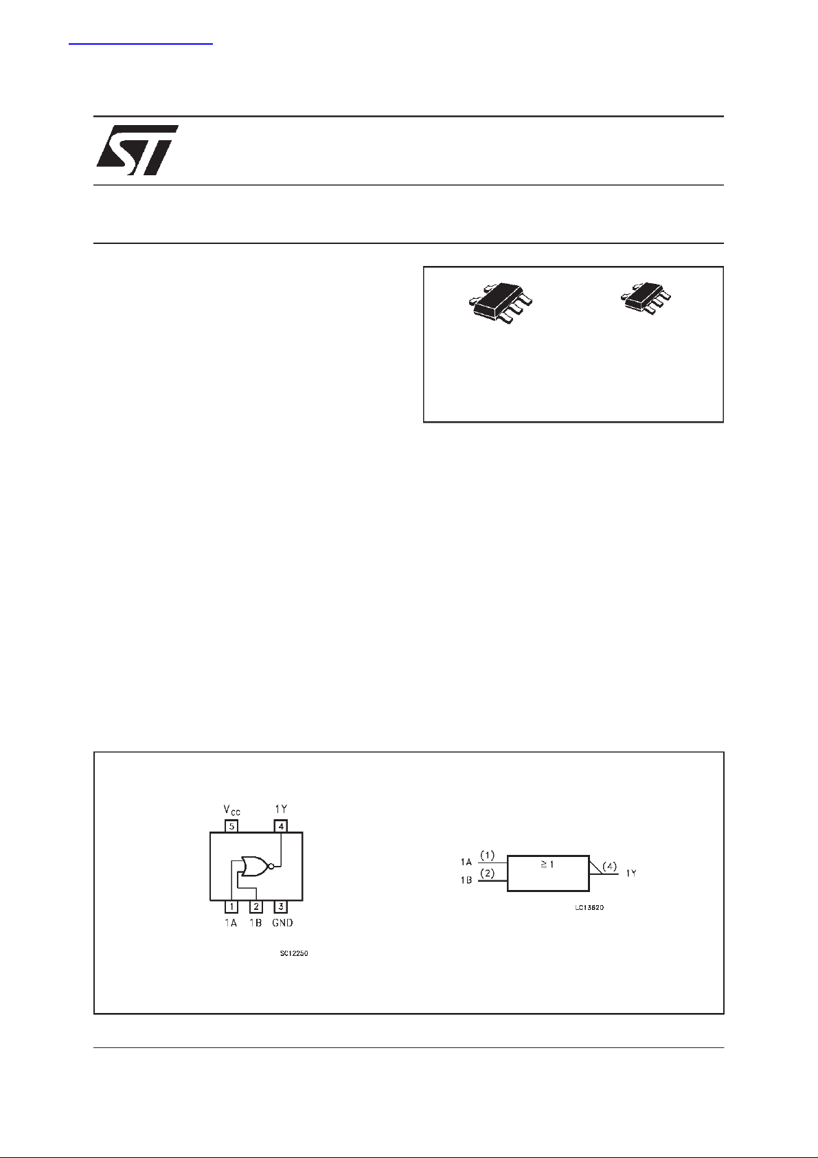
74V1G02
SINGLE 2-INPUT NOR GATE
S
(SOT23-5L)
ORDERCODE:
74V1G02S 74V1G02C
The internal circuit is composed of 3 stages
including buffer output, which provide high noise
immunityandstable output.
Power down protection is provided on all inputs
and 0 to 7V can be accepted on inputs with no
regard to the supply voltage. This device can be
used to interface 5V to 3V.
C
(SC-70)
PIN CONNECTION AND IEC LOGICSYMBOLS
October 1999
1/7
74V1G02
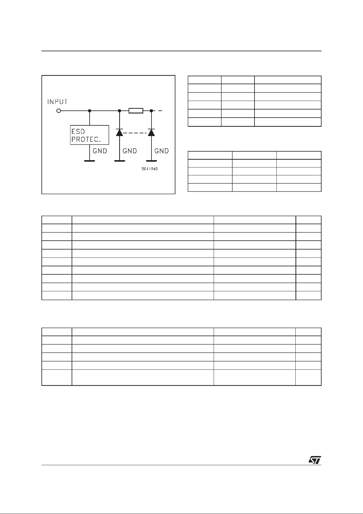
INPUT EQUIVALENTCIRCUIT
PIN DESCRIPTION
PI N No SYMB OL NAME AND F UNCTI O N
1 1A Data Input
2 1B Data Input
4 1Y Data Output
3 GND Ground (0V)
5V
CC
Positive Supply Voltage
TRUTH TABLE
ABY
LLH
LHL
HLL
HHL
ABSOLUTE MAXIMUM RATINGS
Symb o l Para met er Val u e Uni t
V
V
V
I
I
OK
I
or I
I
CC
T
T
AbsoluteMaximum Ratingsarethosevaluesbeyond whichdamagetothedevicemayoccur. Functional operationundertheseconditionisnotimplied.
Supply Voltage -0.5 to +7.0 V
CC
DC Input Voltage -0.5 to +7.0 V
I
DC Output Voltage -0.5 to VCC+ 0.5 V
O
DC Input Diode Current - 20 mA
IK
DC Output Diode Current ± 20 mA
DC Output Current ± 25 mA
O
DC VCCor Ground Current ± 50 mA
GND
Storage Temperature -65 to +150
stg
Lead Temperature (10 sec) 260
L
o
C
o
C
RECOMMENDEDOPERATING CONDITIONS
Symb o l Para met er Value Un it
V
V
V
T
dt/dv
1)VINfrom30%to70%of V
2/7
Supply Voltage 2.0 to 5.5 V
CC
Input Voltage 0 to 5.5 V
I
Output Voltage 0 to V
O
Operating Temperature -40 to +85
op
(V
CC
CC
=3.3±0.3V)
=5.0±0.5V)
Input Rise and Fall Time (see note 1) (V
CC
CC
0 to 100
0to20
V
o
C
ns/V
ns/V
74V1G02
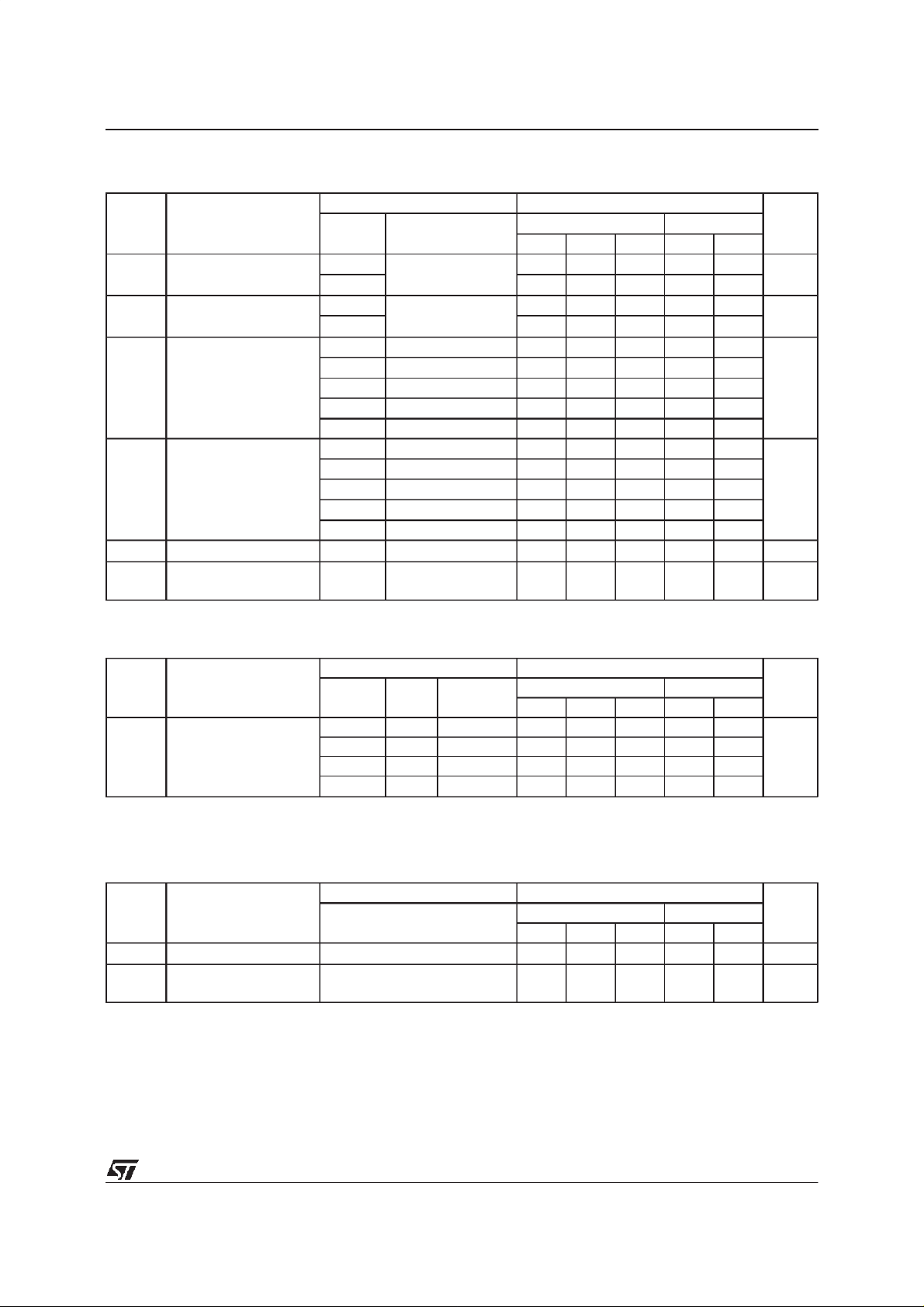
DC SPECIFICATIONS
Symb o l Para met er Test C o n ditio ns Val u e Uni t
T
V
CC
(V)
High Level Input
V
IH
Voltage
V
Low Level Input
IL
Voltage
V
High Level Output
OH
Voltage
Low Level Output
V
OL
Voltage
Input Leakage Current 0 to 5.5 VI= 5.5V or GND ±0.1 ±1.0 µA
I
I
Quiescent Supply
I
CC
2.0 1.5 1.5
3.0 to 5.5 0.7V
2.0 0.5 0.5
3.0 to 5.5 0.3V
2.0 IO=-50 µA 1.9 2.0 1.9
3.0 I
4.5 I
3.0 I
4.5 I
=-50µA 2.9 3.0 2.9
O
=-50µA 4.4 4.5 4.4
O
=-4 mA 2.58 2.48
O
=-8 mA 3.94 3.8
O
2.0 IO=50 µA 0.0 0.1 0.1
3.0 I
4.5 I
3.0 I
4.5 I
=50µA 0.0 0.1 0.1
O
=50µA 0.0 0.1 0.1
O
=4 mA 0.36 0.44
O
=8 mA 0.36 0.44
O
5.5 VI=VCCorGND 1 10 µA
Min. Typ. Max. Min. Max.
Current
=25oC -40 to 85oC
A
CC
0.7V
CC
CC
0.3V
CC
V
V
V
V
AC ELECTRICAL CHARACTERISTICS (Inputtr=tf=3 ns)
Symbol Parameter Test Condition Value Unit
t
Propagation Delay
PLH
t
Time
PHL
(*) Voltagerangeis3.3V± 0.3V
(**) Voltagerange is5V± 0.5V
V
3.3
3.3
5.0
5.0
CC
(V)
(**)
(**)
C
L
(pF)
(*)
15 5.6 8.0 1.0 9.5
(*)
50 8.1 11.4 1.0 13.0
T
=25oC -40 to 85oC
A
Min. Typ. Max. Min. Max.
15 3.6 5.5 1.0 6.5
50 5.1 7.5 1.0 8.5
ns
CAPACITIVE CHARACTERISTICS
Symb o l Para met er Test C o n ditio ns Val u e Uni t
=25oC -40 to 85oC
T
A
Min. Typ. Max. Min. Max.
Input Capacitance 4 10 10
C
IN
Power Dissipation
C
PD
15 pF
Capacitance (note 1)
1)CPDisdefinedasthevalue oftheIC’sinternalequivalentcapacitance whichiscalculatedfromtheoperating currentconsumption without load. (Referto
TestCircuit).Averageoperatingcurrentcanbeobtainedbythefollowingequation.I
(opr)=CPD• VCC• fIN+I
CC
CC
pF
3/7
 Loading...