

Features
■ 5 V tolerant inputs
■ High speed: t
■ Low power dissipation:
–I
■ Power down protection on inputs and outputs
■ Operating voltage range:
–V
■ Latch-up performance exceeds 300 mA
=10μA (max.) at TA=85°C
CC
(opr) = 1.65 to 5.5 V
CC
(JESD 17)
■ ESD performance
– 2000-V human body model
(JESD 22 A114-A)
– 200-V machine model
(JESD 22 A115-A)
– 1000-V charge device model
(JESD 22 C101)
Applications
■ Mobile phones
= 3.7 ns (max.) at VCC= 3.3 V
PD
74LX3G07
Triple buffer/driver with open drain
Flip-chip 8
Description
The 74LX3G07 is a low voltage CMOS triple
buffer/driver (open drain) fabricated with submicron silicon gate and double-layer metal wiring
2
C
MOS technology.
The internal circuit composed of 2 stages
including buffer output, provides high noise
immunity and stable output.
Power down protection is provided on input and 0
to 7 V can be accepted on input with no regards
to the supply voltage. This device can be used to
interface 5 to 3 V.
Table 1. Device summary
Order code Package Packaging
74LX3G07BJR Flip-chip 8 Tape and reel
March 2009 Rev 2 1/14
www.st.com
14
Pin connection 74LX3G07
1 Pin connection
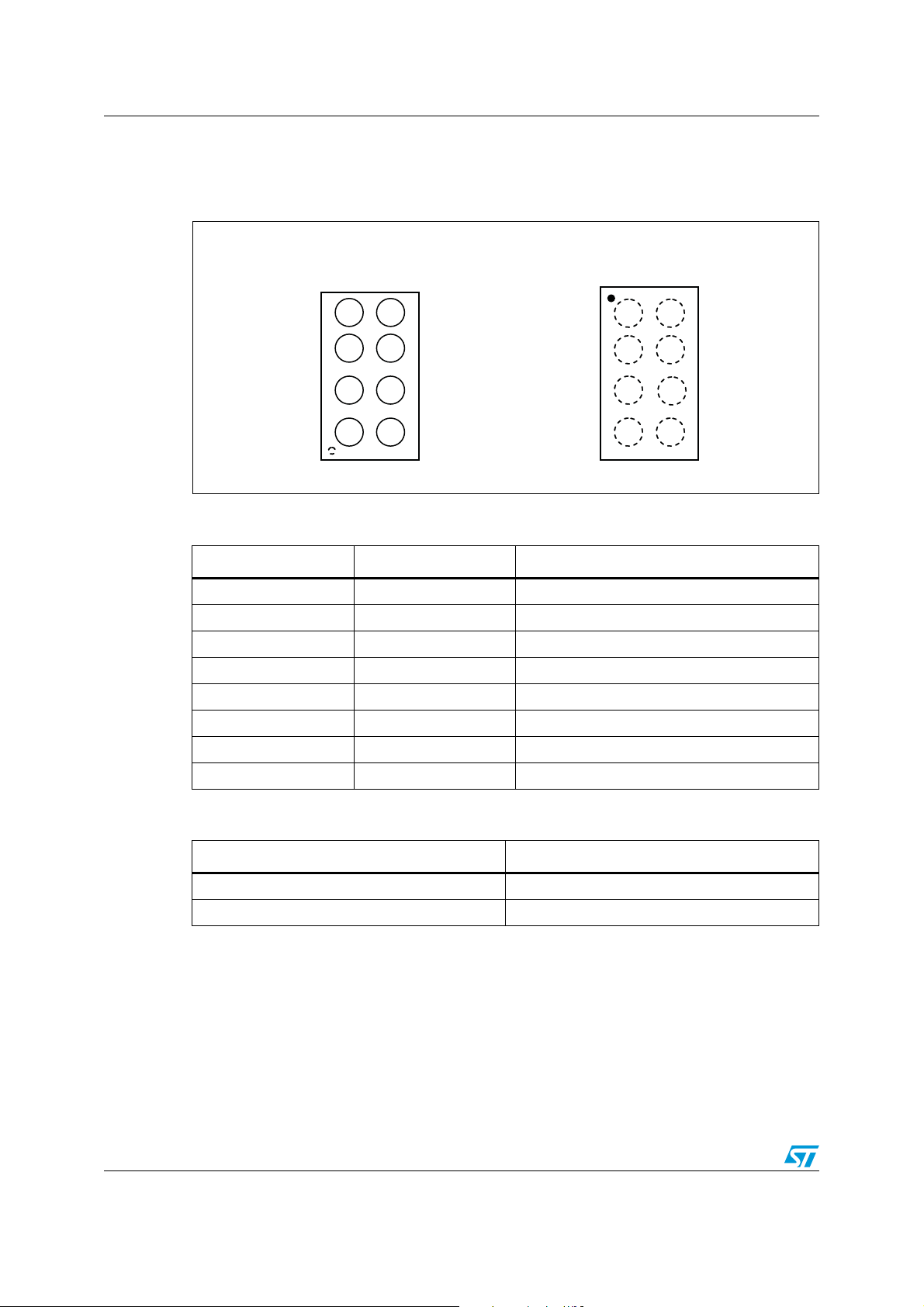
Figure 1. Pin connection and IEC symbols
Bump view Top view
GND
2A
3Y
1A
4
5
3
2
1
2Y
3A
6
7
1Y
V
8
C
C
1A
3Y
2A
GND
1
2 7
3
4 5
Table 2. Pin assignments
Pin number Symbol Name and function
1 1A Data input 1
2 3Y Data output 3
3 2A Data input 2
4 GND Ground (0V)
5 2Y Data output 2
6 3A Data input 3
7 1Y Data output 1
8
6
V
C
C
1Y
3A
2Y
8V
CC
Table 3. Truth table
nA nY
LL
HZ
Z: High impedance
2/14
Positive supply voltage
74LX3G07 Pin connection
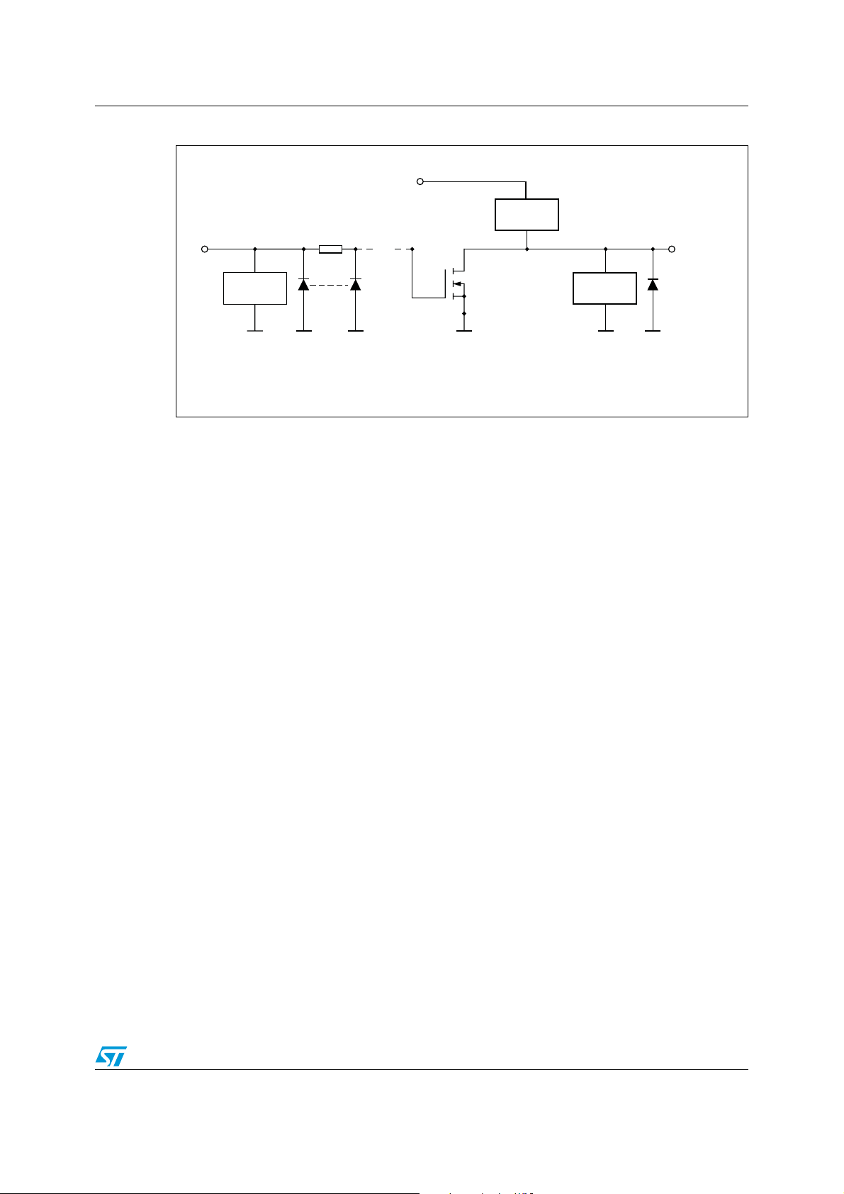
Figure 2. Input and output equivalent circuit
V
CC
Overvoltage
control
Input
Output
ESD
protection
GND GND GND
ESD
protection
GND
GND
CS08973
3/14
Maximum rating 74LX3G07
2 Maximum rating
Stressing the device above the rating listed in the “Absolute maximum ratings” table may
cause permanent damage to the device. These are stress ratings only and operation of the
device at these or any other conditions above those indicated in the operating sections of
this specification is not implied. Exposure to absolute maximum rating conditions for
extended periods may affect device reliability.
Table 4. Absolute maximum ratings
Symbol Parameter Value Unit
V
V
V
V
I
I
OK
I
I
CC
I
GND
T
T
Supply voltage -0.5 to +7.0 V
CC
DC input voltage -0.5 to +7.0 V
I
DC output voltage (VCC= 0 V) -0.5 to +7.0 V
O
DC output voltage (high or low state) -0.5 to VCC + 0.5 V
O
DC input diode current - 50 mA
IK
DC output diode current - 50 mA
DC output current ± 50 mA
O
DC supply current per supply pin ± 100 mA
DC ground current per supply pin ± 100 mA
Storage temperature -65 to +150 °C
stg
Lead temperature (10 sec) 300 °C
L
4/14
74LX3G07 Maximum rating
2.1 Recommended operating conditions
Table 5. Recommended operating conditions
Symbol Parameter Value Unit
V
V
V
I
I
I
I
I
T
Supply voltage 1.65 to 5.5 V
CC
V
Input voltage 0 to 5.5 V
I
Output voltage (VCC= 0 V) 0 to 5.5 V
O
Output voltage (high or low state) 0 to V
O
High or low level output current (VCC= 4.5 to 5.5 V) + 32 mA
OL
High or low level output current (VCC= 3.0 to 3.6 V) +24 mA
OL
High or low level output current (VCC= 2.7 to 3.0 V) +12mA
OL
High or low level output current (VCC= 2.3 to 2.7 V) +8mA
OL
High or low level output current (VCC= 1.65 to 2.3 V) +4mA
OL
Operating temperature -40 to 85 °C
op
CC
V
dt/dv Input rise and fall time 0 to 10 ns/V
5/14

Electrical characteristics 74LX3G07
3 Electrical characteristics
Table 6. DC specifications
Test condition Value
Symbol Parameter
V
V
V
High level input
IH
voltage
Low level input
IL
voltage
Low level output
OL
voltage
High impedance
I
OZ
output leakage
current
Input leakage
I
I
current
I
I
CC
Power off leakage
off
current
Quiescent supply
current
V
CC
(V)
1.65 − 1.95 0.65 V
3.0 − 5.5 0.7 V
1.65 − 1.95 0.35 V
3.0 −5.5 0.3 V
− 4.5 I
1.65
1.65 I
2.3 I
3.0
4.5 I
= 100 μA0.1
O
= 4 mA 0.45
O
=8mA 0.3
O
I
=16mA 0.4
O
=24mA 0.55
I
O
=32mA 0.55
O
-40 to 85 °C
Min Max
CC
CC
CC
CC
CC
CC
3.6 VI= 5.5 V ±10 μA
− 5.5 V
1.65
0V
1.65
− 5.5 V
3.6
=0−5.5 V ±5 μA
I
or VO=5.5V 10 μA
I
or GND 10
I=VCC
or VO= 3.6 to
V
I
5.5 V
±10
Unit
V2.3 −2.7 0.7 V
V2.3 −2.7 0.3 V
V
μA
6/14

74LX3G07 Electrical characteristics
Table 7. AC electrical characteristics
Test conditions Value
Symbol Parameter
V
(V)
CC
C
(pF)
R
t
L
(Ω)
= t
1
s
(ns)
-40 to 85 °C
r
Min Max
1.65 −1.95 30 1000 2.0 1.5 7.8
2.3
t
PLZ
Propagation delay
time
− 2.7 30 500 2.0 1.0 4.3
− 3.6 50 500 2.5 1.1 3.7
3.0
4.5
− 5.5 50 500 2.5 1.0 2.9
1.65 −1.95 30 1000 2.0 1.5 7.8
2.3
t
PZL
Table 8. Capacitive characteristics
Propagation delay
time
− 2.7 30 500 2.0 1.0 4.3
3.0
− 3.6 50 500 2.5 1.1 3.7
−5.5 50 500 2.5 1.0 2.9
4.5
Test conditions Value
Symbol Parameter
C
C
C
Input capacitance 3.3 VIN=0 or V
IN
Output capacitance 3.3 VIN=0 or V
OUT
Power dissipation
PD
capacitance
(1)
V
(V)
1.8
CC
f
=10MHz
IN
CC
CC
TA=25 °C
Min Typ Max
2.5 pF
4pF
8
3.3 8
1. CPD is defined as the value of the IC’s internal equivalent capacitance which is calculated from the
operating current consumption without load. (Refer to test circuit). Average operating current can be
obtained by the following equation: I
CC(opr)=CPDxVCCxfIN+ICC
Unit
ns
ns
Unit
pF2.5 8
7/14

Electrical characteristics 74LX3G07
Figure 3. Test circuit
V
V
CC
CC
R
1
Pulse generator
D.U. T
R
T
C
L
Table 9. Test circuit and waveform symbol value
V
CC
Symbol
1.65 − 1.95 V 2.3 − 2.7 V 2.7 − 5.5 V
C
L
30 pF 30 pF/ 50 pF 50 pF
R1 1000 Ω 500 Ω 500 Ω
V
V
t
r =tf
IH
M
V
CC
VCC/2 VCC/2 VCC/2
<2.0ns <2.0ns <2.5ns
V
CC
Figure 4. Waveform: propagation delay (f = 1 MHz; 50% duty cycle)
V
CS07201
CC
nA
ny
8/14

74LX3G07 Package mechanical data
4 Package mechanical data
In order to meet environmental requirements, ST offers these devices in different grades of
ECOPACK
®
packages, depending on their level of environmental compliance. ECOPACK
®
specifications, grade definitions and product status are available at: www.st.com.
ECOPACK
® is an ST trademark.
Figure 5. Flip-chip 8 package outline
1. Drawing not to scale.
9/14

Package mechanical data 74LX3G07
Table 10. Flip-chip 8 mechanical data
Millimeters
Symbol
Min Typ Max
A 0.535 0.58 0.625
A1 0.18 0.205 0.23
A2 0.355 0.375 0.395
b 0.215 0.255 0.295
D 1.85 1.9 1.95
D1 1.5
e 0.45 0.5 0.55
E 0.85 0.9 0.95
E1 0.45 0.5 0.55
SE 0.25
f 0.19 0.2 0.21
ccc 0.08
Figure 6. Flip-chip 8 footprint
GRID PLACEMENT AREA
A
B
1.5
0.5
12
3
0.5
4
0.22
10/14

74LX3G07 Package mechanical data
Figure 7. Flip-chip 8 tape and reel
Figure 8. Tape orientation
5SERDIRECTIONOFFEED
!-6
!-6
11/14

Package mechanical data 74LX3G07
Figure 9. Reel information
12/14

74LX3G07 Revision history
5 Revision history
Table 11. Document revision history
Date Revision Changes
10-Jul-2008 1 Initial release.
19-Mar-2009 2
Preliminary status promoted to datasheet. Updated Section 4:
Package mechanical data.
13/14

74LX3G07
Please Read Carefully:
Information in this document is provided solely in connection with ST products. STMicroelectronics NV and its subsidiaries (“ST”) reserve the
right to make changes, corrections, modifications or improvements, to this document, and the products and services described herein at any
time, without notice.
All ST products are sold pursuant to ST’s terms and conditions of sale.
Purchasers are solely responsible for the choice, selection and use of the ST products and services described herein, and ST assumes no
liability whatsoever relating to the choice, selection or use of the ST products and services described herein.
No license, express or implied, by estoppel or otherwise, to any intellectual property rights is granted under this document. If any part of this
document refers to any third party products or services it shall not be deemed a license grant by ST for the use of such third party products
or services, or any intellectual property contained therein or considered as a warranty covering the use in any manner whatsoever of such
third party products or services or any intellectual property contained therein.
UNLESS OTHERWISE SET FORTH IN ST’S TERMS AND CONDITIONS OF SALE ST DISCLAIMS ANY EXPRESS OR IMPLIED
WARRANTY WITH RESPECT TO THE USE AND/OR SALE OF ST PRODUCTS INCLUDING WITHOUT LIMITATION IMPLIED
WARRANTIES OF MERCHANTABILITY, FITNESS FOR A PARTICULAR PURPOSE (AND THEIR EQUIVALENTS UNDER THE LAWS
OF ANY JURISDICTION), OR INFRINGEMENT OF ANY PATENT, COPYRIGHT OR OTHER INTELLECTUAL PROPERTY RIGHT.
UNLESS EXPRESSLY APPROVED IN WRITING BY AN AUTHORIZED ST REPRESENTATIVE, ST PRODUCTS ARE NOT
RECOMMENDED, AUTHORIZED OR WARRANTED FOR USE IN MILITARY, AIR CRAFT, SPACE, LIFE SAVING, OR LIFE SUSTAINING
APPLICATIONS, NOR IN PRODUCTS OR SYSTEMS WHERE FAILURE OR MALFUNCTION MAY RESULT IN PERSONAL INJURY,
DEATH, OR SEVERE PROPERTY OR ENVIRONMENTAL DAMAGE. ST PRODUCTS WHICH ARE NOT SPECIFIED AS "AUTOMOTIVE
GRADE" MAY ONLY BE USED IN AUTOMOTIVE APPLICATIONS AT USER’S OWN RISK.
Resale of ST products with provisions different from the statements and/or technical features set forth in this document shall immediately void
any warranty granted by ST for the ST product or service described herein and shall not create or extend in any manner whatsoever, any
liability of ST.
ST and the ST logo are trademarks or registered trademarks of ST in various countries.
Information in this document supersedes and replaces all information previously supplied.
The ST logo is a registered trademark of STMicroelectronics. All other names are the property of their respective owners.
© 2009 STMicroelectronics - All rights reserved
STMicroelectronics group of companies
Australia - Belgium - Brazil - Canada - China - Czech Republic - Finland - France - Germany - Hong Kong - India - Israel - Italy - Japan -
Malaysia - Malta - Morocco - Singapore - Spain - Sweden - Switzerland - United Kingdom - United States of America
www.st.com
14/14
 Loading...