

查询74LX1G14供应商
LOW VOLTAGE CMOS SINGLE SCHMITT INVERTER
■ 5V TOLERANT INPUTS
■ HIGH SPEED:t
■ LOW POWER DISSIPATION:
I
=1µA(MAX.)atTA=25°C
CC
■ TYPICAL HYSTERESIS: V
■ POWER DOWN PROTECTION ON INPUTS
AND OUTPUTS
■ SYMMETRICAL OUTPUT IMPEDANCE:
|I
|=IOL= 24mA (MIN) at VCC=3V
OH
■ BALANCED PROPAGATION DELAYS:
t
≅ t
PLH
PHL
■ OPERATING VOLTAGE RANGE:
V
(OPR) = 1.65V to 5.5V
CC
(1.2V Data Retention)
■ IMPROVED LATCH-UP IMMUNITY
DESCRIPTION
The 74LX 1G14 is a low voltag e CMOS SING LE
SCHMITT INVERTER f abricated with sub-micron
silicon gate and double -layer metal wiring C
technology.
It is ideal f or 1.65 to 5.5 V
power and low noise applications. The internal
circuit is composed of 3 stages including buffer
output, which provide high noise immunity and
stable output.
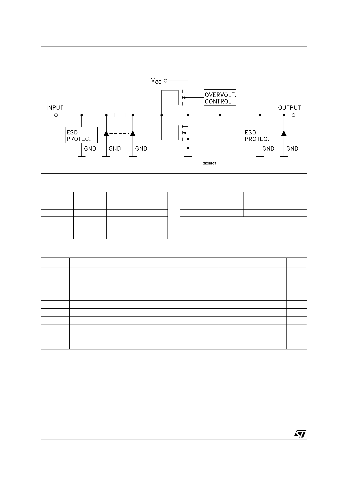
Powerdownprotectionisprovidedoninputand
output and 0 to 7V can be accepted on inputs with
= 7. 5ns (MAX.) at VCC=3V
PD
=1V at VCC=4.5V
h
operations and low
CC
2
MOS
74LX1G14
WITH 5V TOLERANT INPUT
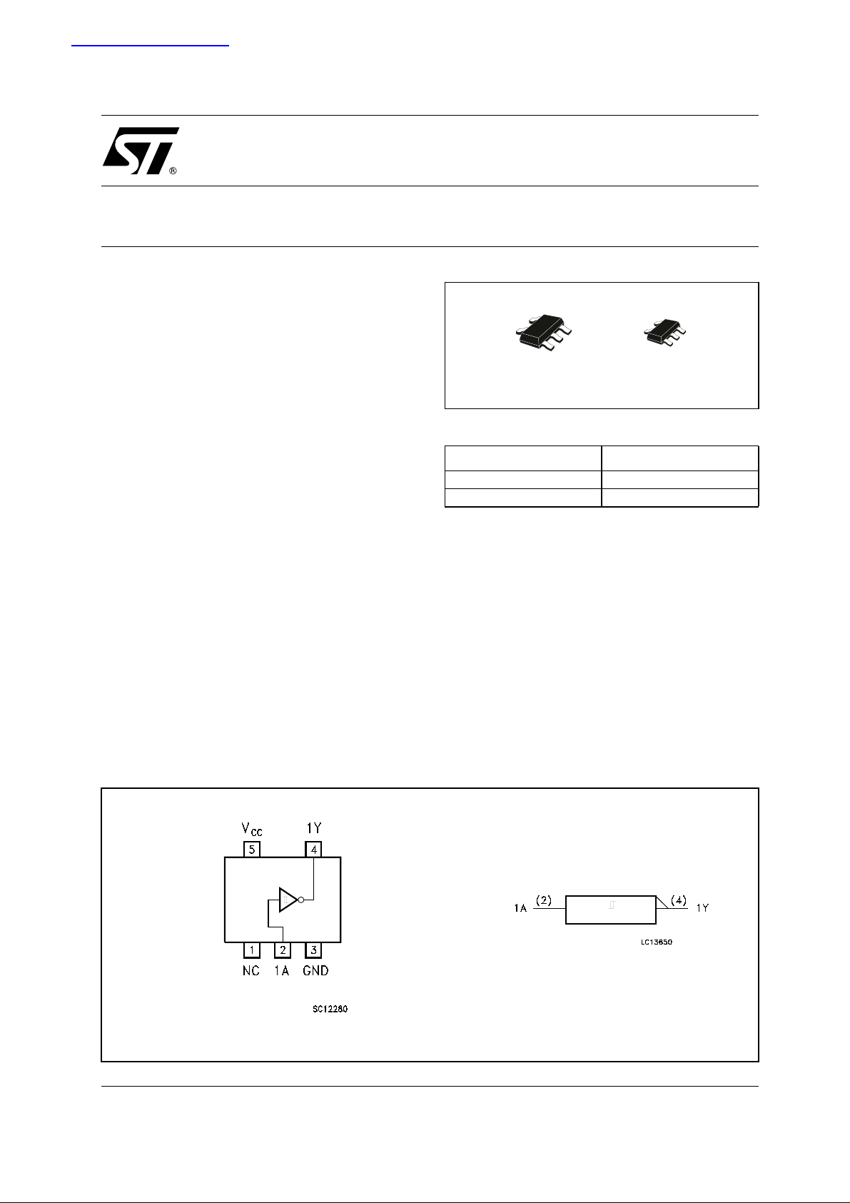
SOT323-5LSOT23-5L
ORDER CODES
PACKAGE T & R
SOT23-5L 74LX1G14STR
SOT323-5L 74LX1G14CTR
no regard to the supply voltage. It c an be
interfaced t o 5V signal environment for inputs in
mixed 3.3/5V system.
Pin configuration and func tion are the same as
those of the 74LX1G04 but the 74LX1G14 has
hysteresis.
This together with its schmitt trigger function
allows it to be used on line receivers with slow
rise/fall input signals.
The input is equipped with protection circuits
against static discharge, giving it ESD immunity
and transient excess voltage.
PIN CONNECTION AND IEC LOGIC SYMBOLS
1/11December 2002
74LX1G14
INPUT AND O UTPUT EQUIVALENT CIRCUIT
PIN DESCRIPTION TRUTH TABLE
PIN No SYMBOL NAME AND FUNCTION
1 NC Not Connected
2 1A Data Input
AY
LH
HL
4 1Y Data Output
3 GND Ground (0V)
5
V
CC
Positive Supply Voltage
ABSOLUTE MAXIMUM RATINGS
Symbol Parameter² Value Unit
V
V
V
V
I
I
OK
I
or I
I
CC
T
T
Absolute Maximum Ratings are those values beyond which damage to the device may occur. Functional operation under these conditions is
not implied.
1) Truth Table guaranteed: 1.2V to 3.6V
2) V
from0.8V to 2V at VCC=3.0V
IN
Supply Voltage
CC
DC Input Voltage
I
DC Output Voltage (VCC= 0V)
O
DC Output Voltage (High or Low State) (note 1) -0.5 to VCC+ 0.5
O
DC Input Diode Current
IK
DC Output Diode Current (note 2)
DC Output Current
O
DC VCCor Ground Current per Supply Pin
GND
Storage Temperature
stg
Lead Temperature (10 sec)
L
-0.5 to +7.0 V
-0.5 to +7.0 V
-0.5 to +7.0 V
V
-50 mA
-50 mA
± 50 mA
± 50 mA
-65 to +150 °C
300 °C
2/11
74LX1G14
RECOMMENDED OPERATING CONDITIONS
Symbol Parameter Value Unit
V
V
V
V
I
OH,IOL
I
OH,IOL
I
OH,IOL
I
OH,IOL
I
OH,IOL
T
1) Truth Table guaranteed: 1.2V to 3.6V
2) V
from0.8V to 2V atVCC=3.0V
IN
Supply Voltage (note 1)
CC
Input Voltage
I
Output Voltage (VCC= 0V)
O
Output Voltage (High or Low State) 0 to V
O
High or Low Level Output Current (VCC= 4.5 to 5.5V)
High or Low Level Output Current (VCC= 3.0 to 3.6V)
High or Low Level Output Current (VCC= 2.7 to 3.0V)
High or Low Level Output Current (VCC= 2.3 to 2.7V)
High or Low Level Output Current (VCC= 1.65 to 2.3V)
Operating Temperqture
op
1.65 to 5.5 V
0to5.5 V
0to5.5 V
CC
± 32 mA
± 24 mA
± 12 mA
± 8mA
± 4mA
-55 to 125 °C
V
3/11
74LX1G14
DC SPECIFICATIONS
Test Condition Value
Symbol Parameter
V
V
V
I
Positive Input
T+
threshold
V
Negative Input
T-
threshold
High Level Output
OH
Voltage
Low Level Output
OL
Voltage
Hysteresis Voltage 1.65 0.37 0.62 0.37 0.62
V
H
I
Input Leakage
I
Current
I
Power Off Leakage
off
Current
Quiescent Supply
CC
Current
V
CC
(V)
-40 to 85 °C -55 to 125 °C
Min. Max. Min. Max.
1.65 0.79 1.16 0.79 1.16
2.3 1.11 1.56 1.11 1.56
3 1.5 1.87 1.5 1.87
4.5 2.16 2.74 2.16 2.74
5.5 2.61 3.33 2.61 3.33
1.65 0.39 0.62 0.39 0.62
2.3 0.58 0.87 0.58 0.87
3 0.84 1.14 0.84 1.14
4.5 1.41 1.79 1.41 1.79
5.5 1.87 2.29 1.87 2.29
=-100 µAVCC-0.1 VCC-0.1
1.65 to 4.5
1.65
2.3
3.0
4.5
1.65 to 4.5
1.65
2.3
3.0
4.5
I
O
=-4 mA
I
O
=-8 mA
I
O
I
=-16 mA
O
=-24 mA
I
O
=-32 mA
I
O
IO=100 µA
=4 mA
I
O
=8 mA
I
O
I
=16 mA
O
=24 mA
I
O
I
=32 mA
O
1.2 1.2
1.9 1.9
2.4 2.4
2.2 2.2
3.8 3.8
0.1 0.1
0.45 0.45
0.3 0.3
0.4 0.4
0.55 0.55
0.55 0.55
2.3 0.48 0.77 0.48 0.77
3 0.56 0.87 0.56 0.87
4.5 0.71 1.04 0.71 1.04
5.5 0.71 1.11 0.71 1.11
= 0 to 5.5V
1.65 to 5.5
0
1.65 to 5.5
V
I
or VO= 5.5V
V
I
V
I=VCC
or GND
± 10 ±10 µA
10 10 µA
10 10 µA
Unit
V
V
V
V
V
4/11
 Loading...