

LOW VOLTAGE CMOS SINGLE INVERTER
■ 5V TOLERANT INPUTS
■ HIGH SPEED: t
■ LOW POWER DISSIPATION:
I
=1µA(MAX.)atTA=25°C
CC
■ POWER DOWN PROTECTION ON INPUTS
AND OUTPUTS
■ SYMMETRICAL OUTPUTIMPEDANCE:
|I
|=IOL= 24mA (MIN) at VCC=3V
OH
■ BALANCED PROPAGATION DELAYS:
t
≅ t
PLH
PHL
■ OPERATING VOLTAGE RANGE:
V
(OPR) = 1.65V to 5.5V
CC
(1.2V Data Reten tion)
■ IMPROVED LATCH-UP IMMUNITY
= 4.2ns (MAX.) at VCC=3V
PD
74LX1G04
WITH 5V TOLERANT INPUT
SOT23-5 SOT323-5
Flip-Chip4
DESCRIPTION
The 74LX1G04 is a low voltage CMOS SINGLE
INVERTER fabricated with sub-micron silicon
gate and double-layer metal wi ring C
2
MOS
technology.
It is ideal f or 1.65 to 5.5 V
operations and low
CC
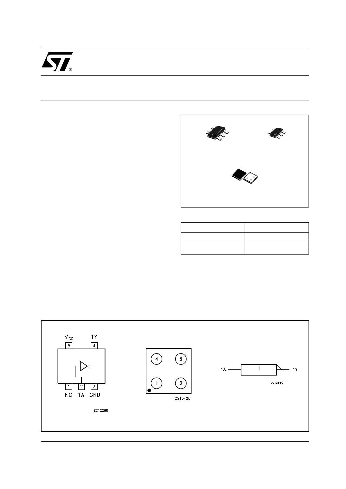
ORDER CODES
PACKAGE T & R
SOT23-5L 74LX1G04STR
SOT323-5L 74LX1G04CTR
Flip-Chip 74LX1G04BJR
power and low noise a pplications. The internal
circuit is composed of 3 stages including buffer
output, which provide high noise immunity and
stable output.
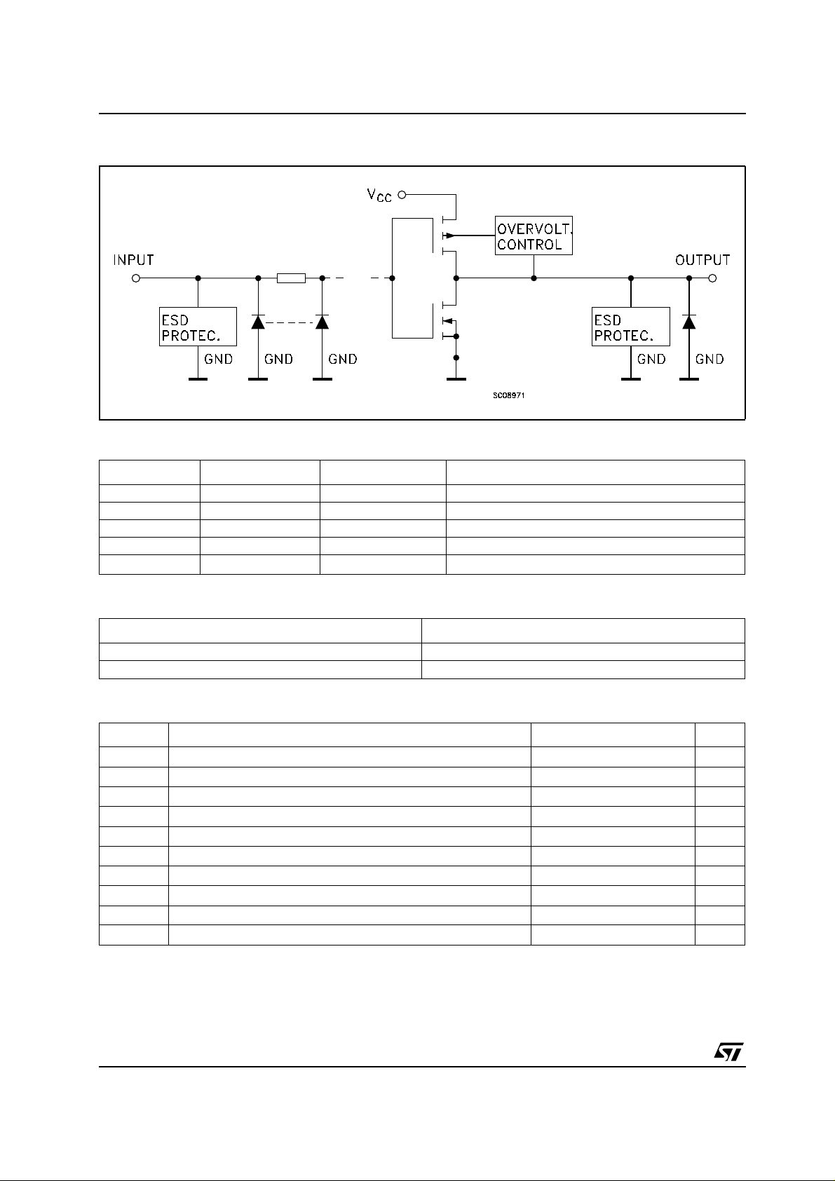
Powerdownprotectionisprovidedoninputand
output and 0 to 7V can be accepted on inputs with
no regard to the supp ly voltage. It can be
interfaced to 5V signal e nvironment for inputs in
mixed 3.3/5V system.
All inputs and outputs are equipped with
protection circuits against static discharge.
PIN CONNECTION AND IEC LOGIC SYMBOLS (top view for S OT, top through view for Flip-Chip)
1/13April 2004
74LX1G04
INPUT AND OUTPUT EQUIVALENT CIRCUIT
PIN DESCRIPTION
PIN for SOT PIN for Flip-Chip SYMBOL NAME AND FUNCTION
1 N.C. Not connected
2 1 1A Data Input
4 3 1Y Data Output
3 2 GND Ground (0V)
54
V
CC
Positive Supply Voltage
TRUTH TABLE
AY
LH
HL
ABSOLUTE MAXIMUM RATINGS
Symbol Parameter Value Unit
V
V
V
V
I
I
OK
I
or I
I
CC
T
T
Absolute Maximum Rating are those value beyond which damage to the device may occur. Functional operation under these condition is not
implied
1) I
absolute maximum rating must be observed
O
2) V
<GND
O
Supply Voltage
CC
DC Input Voltage
I
DC Output Voltage (VCC=0V)
O
DC Output Voltage (High or Low State) (note 1) -0.5 to VCC+0.5
O
DC Input Diode Current
IK
DC Output Diode Current (note 2)
DC Output Current
O
DC VCCor Ground Current per Supply Pin
GND
Storage Temperature
stg
Lead Temperature (10 sec)
L
-0.5 to +7.0 V
-0.5 to +7.0 V
-0.5 to +7.0 V
V
-50 mA
-50 mA
± 50 mA
± 50 mA
-65 to +150 °C
260 °C
2/13
74LX1G04
RECOMMENDED OPERATING CONDITIONS
Symbol Parameter Value Unit
V
V
V
V
I
OH,IOL
I
OH,IOL
I
OH,IOL
I
OH,IOL
I
OH,IOL
T
dt/dv Input Rise and Fall Time (note 2) 0 to 10 ns/V
1) Truth Table guaranteed: 1.2V to 3.6V
2) V
from0.8V to 2V at VCC=3.0V
IN
DC SPECIFICATION
Supply Voltage (note 1)
CC
Input Voltage
I
Output Voltage (VCC=0V)
O
Output Voltage (High or Low State) 0 to V
O
High or Low Level Output Current (VCC=4.5to5.5V)
High or Low Level Output Current (VCC=3.0to3.6V)
High or Low Level Output Current (VCC=2.7to3.0V)
High or Low Level Output Current (VCC=2.3to2.7V)
High or Low Level Output Current (VCC=1.65to2.3V)
Operating Temperature
op
Test Condition Value
1.65 to 5.5 V
0to5.5 V
0to5.5 V
CC
± 32 mA
± 24 mA
± 16 mA
± 8mA
± 4mA
-55 to 125 °C
V
Symbol Parameter
V
V
V
High Level Input
IH
Voltage
V
Low Level Input
IL
Voltage
High Level Output
OH
Voltage
Low Level Output
OL
Voltage
Input Leakage
I
I
Current
I
Power Off Leakage
off
Current
Quiescent Supply
I
CC
Current
V
CC
(V)
1.65 to 1.95
3.0 to 5.5
1.65 to 1.95
3.0 to 5.5
1.65to4.5
1.65
2.3
3.0
4.5
1.65to4.5
1.65
2.3
3.0
4.5
1.65to5.5
0
1.65to5.5
-40 to 85 °C -55 to 125 °C
Min. Max. Min. Max.
0.75V
0.7V
0.7V
CC
CC
CC
0.25V
0.3V
0.3V
0.75V
CC
CC
CC
IO=-100 µAVCC-0.1 VCC-0.1
=-4 mA
I
O
I
=-8 mA
O
I
=-16 mA
O
I
=-24 mA
O
=-32 mA
I
O
IO=100 µA
=4 mA
I
O
I
=8 mA
O
I
=16 mA
O
I
=24 mA
O
=32 mA
I
O
= 0 to 5.5V
V
I
V
or VO=5.5V
I
V
I=VCC
or GND
1.2 1.2
1.9 1.9
2.4 2.4
2.2 2.2
3.8 3.8
0.1 0.1
0.45 0.45
0.3 0.3
0.4 0.4
0.55 0.55
0.55 0.55
± 10 ± 10 µA
10 10 µA
10 10 µA
0.7V
0.7V
CC
CC
CC
0.25V
0.3V
0.3V
CC
CC
Unit
V2.3 to 2.7
CC
V2.3 to 2.7
V
V
3/13
74LX1G04
AC ELECTRICAL CHARACTERISTICS
Test Condition Value
Symbol Parameter
t
PLHtPHL
Propagation Delay
Time
V
(V)
CC
C
(pF)
R
L
(Ω)
= t
t
L
s
(ns)
1.65 to 1.95
2.3to2.7 26.527.6
3.0to3.6 15.516.5
15 1MΩ 2.0
-40to85°C -55to125°C
r
Min. Max. Min. Max.
29.5210.5
Unit
4.5to5.5 14.115.5
1.65 to 1.95 30 1000 2.0 2 10.5 2 11.5
ns
2.3 to 2.7 30 500 2.0 2 7.5 2 8.5
2.7 50 500 2.5 1 6.1 1 7.1
3.0 to 3.6 50 500 2.5 1 5.5 1 6.5
4.5 to 5.5 50 500 2.5 1 4.2 1 5.2
CAPACITANCE CHARACTERISTICS
Test Condition Value
=25°C
Symbol Parameter
V
CC
(V)
C
C
Input Capacitance
IN
Power Dissipation Capacitance
PD
(note 1)
04pF
1.8 fIN=10MHz 36.8
3.3 38
1) CPDis defined as the value of the IC’s internal equivalent capacitance which is calculated from the operating current consumption without
load. (Refer to Test Circuit). Average current can be obtained by the following equation. I
CC(opr)=CPDxVCCxfIN+ICC
T
A
Min. Typ. Max.
Unit
pF2.5 37
4/13

TEST CIRCUIT
74LX1G04
RT=Z
of pulse generator (typically 50Ω)
OUT
TEST CIRCUIT AND WAVEFORM SYMBOL VALUE
V
Symbol
CC
1.65 to 1.95V 2.3 to 2.7V 2.7 to 5.5V
C
R
V
V
t
r=tr
L
L
IH
M
15pF/30pF 15pF/30pF 15pF/50pF
1MΩ/1000Ω 500Ω 500Ω
V
CC
V
CC
VCC/2 VCC/2 VCC/2
<2.0ns <2.0ns <2.5ns
WAVEFORM: PROPAGATION DELAY (f=1MHz; 50% duty cycle)
V
CC
5/13

74LX1G04
Figure1 : RECO MMENDE D S O LDERING RE F LOW PROFILE FOR LEADFREE FLIP-CHIP
MOUNTING ON PCB
Temperature (˚C)
Temperature (˚C)
260˚C max
260˚C max
255˚C
255˚C
220˚C
220˚C
180˚C
180˚C
125 ˚C
125 ˚C
3˚C/s max
3˚C/s max
0
0
01234567
01234567
10-30 sec
10-30 sec
90 to 150 sec
90 sec max
90 sec max
2˚C/s recommended
2˚C/s recommended
6˚C/s max
6˚C/s max
Time (min)
Time (min)
For Flip-Chip mounting on the PCB, S TM icroelectronics recommends the use of a solder s tenci l aperture
of 330 x 330 µm² maximum and a typical stencil thick nes s of 125µm . Flip-Chips are fully compatible with
the use of near eut ec tic 95.5Sn 4Ag 0.5Cu s older paste with no clean flux. ST's r ec ommendations for
Flip-Chip board mou nting are illustrated on the soldering reflow profile shown in figure 1 below.
Dwell time in th e soldering zone (with temperat ure higher than 220 °C) has to be kept as short as possible
to prevent component and subs trate damages. Peak temperature must not exceed 260°C. Controlled
atmosphere (N2 or N2H2) is recomm ended during the whole reflow, specially above 150°C.
Flip-Chips are able to withstand three time s the previous recommended reflow pro file in order to be
compatible with a double reflow when SMDs are mounted on both sides of the PCB plus one additional
repair. A maximum of three soldering reflows are allo wed f or these leadfree packages (with repair step
included). The use of a no clean flux is highly rec ommended to avoid any cleaning operation. In order to
prevent any bump cracks, ultrasonic cleaning met hods are not recommended.
6/13

74LX1G04
SOT23-5L MECHANICAL DATA
mm. mils
DIM.
MIN. TYP MAX. MIN. TYP. MAX.
A 0.90 1.45 35.4 57.1
A1 0.00 0.10 0.0 3.9
A2 0.90 1.30 35.4 51.2
b 0.35 0.50 13.7 19.7
C 0.09 0.20 3.5 7.8
D 2.80 3.00 110.2 118.1
E 1.50 1.75 59.0 68.8
e0.95 37.4
H 2.60 3.00 102.3 118.1
L 0.10 0.60 3.9 23.6
.
7049676C
7/13

74LX1G04
SOT323-5L MECHANICAL DATA
mm. mils
DIM.
MIN. TYP MAX. MIN. TYP. MAX.
A 0.80 1.10 31.5 43.3
A1 0.00 0.10 0.0 3.9
A2 0.80 1.00 31.5 39.4
b 0.15 0.30 5.9 11.8
C 0.10 0.18 3.9 7.1
D 1.80 2.20 70.9 86.6
E 1.80 2.40 70.9 94.5
E1 1.15 1.35 45.3 53.1
e
e1 1.3 51.2
L 0.10 0.30 3.9 11.8
.65
0
25.6
8/13

74LX1G04
Flip-Chip4 MECHANICAL DATA
mm. mils
DIM.
MIN. TYP MAX. MIN. TYP. MAX.
A 0.585 0.65 0.715 23.03 25.59 28.15
A1 0.21 0.25 0.29 8.27 9.84 11.42
A2 0.40 15.75
b 0.265 0.315 0.365 10.43 12.40 14.37
D 1.02 1.07 1.12 40.15 42.13 44.09
D1 0.5 19.69
E 1.02 1.07 1.12 40.15 42.13 44.09
E1 0.5 19.69
7224716/D
9/13

74LX1G04
Tape & Reel SOT23-xL MECHANICAL DATA
DIM.
MIN. TYP MAX. MIN. TYP. MAX.
A 180 7.086
C 12.8 13.0 13.2 0.504 0.512 0.519
D 20.2 0.795
N 60 2.362
T 14.4 0.567
Ao 3.13 3.23 3.33 0.123 0.127 0.131
Bo 3.07 3.17 3.27 0.120 0.124 0.128
Ko 1.27 1.37 1.47 0.050 0.054 0.0.58
Po 3.9 4.0 4.1 0.153 0.157 0.161
P 3.9 4.0 4.1 0.153 0.157 0.161
mm. inch
10/13

Tape & Reel SOT323-xL MECHANICAL DATA
74LX1G04
DIM.
MIN. TYP MAX. MIN. TYP. MAX.
A 175 180 185 6.889 7.086 7.283
C 12.8 13 13.2 0.504 0.512 0.519
D 20.2 0.795
N 59.5 60 60.5 2.362
T 14.4 0.567
Ao 2.25 0.088
Bo 2.7 0.106
Ko 1.2 0.047
Po 3.9 4 4.1 0.153 0.157 0.161
P 3.8 4 4.2 0.149 0.157 0.165
mm. inch
11/13

74LX1G04
Tape & Reel Flip-Chip 4 MECHANICAL DATA
mm. inch
DIM.
MIN. TYP MAX. MIN. TYP. MAX.
A 178 6.926
C 12.8 13.2 0.504 0.519
D 20.2 0.795
N 59 60 61 2.323 2.362 2.401
T 8.4 0.331
Ao 1.12 1.17 1.22 0.044 0.046 0.048
Bo 1.12 1.17 1.22 0.044 0.046 0.048
Ko 0.68 0.73 0.78 0.027 0.029 0.031
Po 3.9 4 4.1 0.153 0.157 0.161
P 3.9 4 4.1 0.153 0.157 0.161
12/13

74LX1G04
Information furnished is believed to be accurate and reliable. However, STMicroelectronics assumes no responsibility for the
consequences of use of such inform ation nor fo r an y infring ement of p atents or o ther rights of third p arties which may r esult f rom
its use. No license is granted by implication or otherwise under any patent or patent rights of STMicroelectronics. Specifications
mentioned in this publication are subject to change without notice. This publication supersedes and replaces all information
previously supplied. STMicroelectronics products are not authorized for use as critical components in life support devices or
systems without express written approval of STMicroelectronics.
Australia - Belgium - Brazil - Canada - China - Czech Republic - Finland - France - Germany - Hong Kong - India - Israel - Italy - Japan -
Malaysia - Malta - Morocco - Singapore - Spain - Sweden - Switzerland - United Kingdom - United States.
The ST logo is a registered trademark of STMicroelectronics
All other names are the property of their respective owners
© 2004 STMicroelectronics - All Rights Reserved
STMicroelectronics GROUP OF COMPANIES
http://www.st.com
13/13
 Loading...