

74LVXC4245
OCTAL DUAL SUPPLY BUS TRANSCEIVER
■ HIGH SPEED:
t
= 6.5ns (MAX.) at
PD
V
= 5.0V, V
CCA
■ LOW POWER DISSIPATION:
I
= I
CCA
■ LOW NOISE: V
V
CCA
■ SYMMETRICAL OUTPUT IMPEDANCE:
| = IOL = 24mA (MIN)
|I
OH
■ BALANCED PROPAGATION DELAYS:
≅ t
t
PLH
■ OPERATING VOLT AG E R AN GE:
V
CCA
V
CCB
= 5µA(MAX.) at TA=25°C
CCB
=5.0V V
PHL
(OPR) = 4.5V to 5.5V (1.2V Data Retention)
(OPR) = 2.7V to 5.5V (1.2V Data Retention)
= 5.0V
CCB
=0.3V (TYP.) at
OLP
=3.3V
CCB
PIN AND FUNCTION COMPATIBLE WITH
74 SERIES C4245
■ IMPROVED LATCH-UP I MMUN ITY
DESCRIPTION
The 74LVXC4245 is a dual supply 8 bit
configurable low voltage CMOS OCTAL BUS
TRANSCEIVER fabricated with sub-micron silicon
gate and double-layer metal wiring C
2
MOS
technology. Designed for use as an interface
between a 5V bus and a 3.3V to 5V bus in a mixed
5V/3.3V supply systems, it achieves high speed
operation while maintaining the CMOS low power
dissipation.
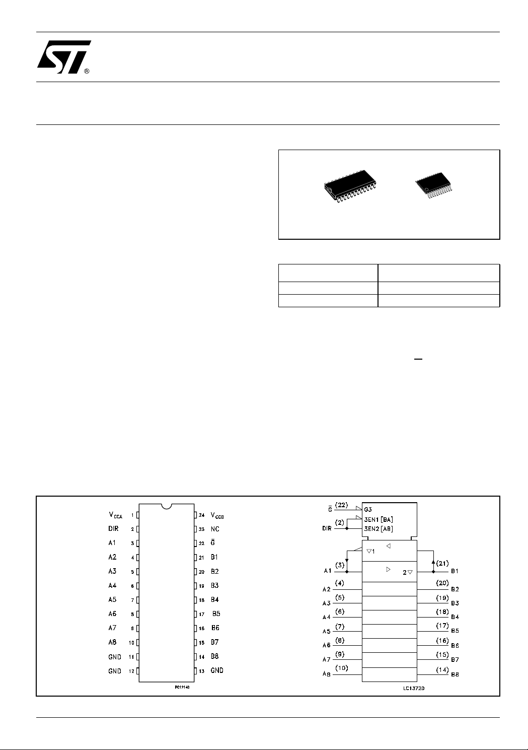
TSSOPSOP
Table 1: Order Codes
PACKAGE T & R
SOP 74LVXC4245MTR
TSSOP 74LVXC4245TTR
This IC is intended for two-way asynchronous
communication between data buses and the
direction of data transmission is determined by
DIR input. The enable input G
can be used to
disable the device so that the buses are effectively
isolated.
The A-port interfaces with the 5V bus, the B-port
with the 3.3V to 5V bus.
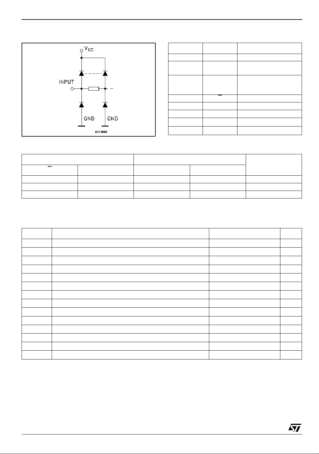
All inputs are equipped with protection circuits
against static discharge, giving them 2KV ESD
immunity and transient excess voltage.
Figure 1: Pin Connection And IEC Logic Symbols
Rev. 4
1/14August 2004
74LVXC4245
Figure 2: Input And Output Equivalent Circuit Table 2: Pin Description
PIN N° SYMBOL NAME AND FUNCTION
2 DIR Directional Control
3, 4, 5, 6, 7,
8, 9, 10
21, 20, 19,
18, 17, 16,
15, 14
22 G
11, 12, 13 GND Ground (0V)
23 NC Not Connected
1V
24 V
Table 3: Truth Tab l e
A1 to A8 Data Inputs/Outputs
B1 to B8 Data Inputs/Outputs
Output Enable Input
CCA
CCB
Positive Supply Voltage
Positive Supply Voltage
INPUTS FUNCTION
OUTPUT
G
DIR A BUS B BUS
L L OUTPUT INPUT A = B
L H INPUT OUTPUT B = A
HXZZZ
X : Don’t Care
Z : High Impedance
Table 4: Absolute maximum ratings
Symbol Parameter Value Unit
V
CCA
V
CCB
V
V
I/OA
V
I/OB
I
I
OK
I
OA
I
OB
I
CCA
I
CCB
P
T
T
Absolute Maximum Ratings are those values beyond which damage to the device may occur. Functional operation under these conditions is
not implied
Supply Voltage
Supply Voltage
DC Input Voltage -0.5 to V
I
DC I/O Voltage -0.5 to V
DC I/O Voltage -0.5 to V
DC Input Diode Current
IK
DC Output Diode Current
DC Output Current
DC Output Current
DC VCC or Ground Current
DC VCC or Ground Current
Power Dissipation
d
Storage Temperature
stg
Lead Temperature (10 sec)
L
-0.5 to +7.0 V
-0.5 to +7.0 V
+ 0.5
CCA
+ 0.5
CCA
+ 0.5
CCB
± 20 mA
± 50 mA
± 50 mA
± 50 mA
± 200 mA
± 100 mA
180 mW
-65 to +150 °C
300 °C
V
V
V
2/14
74LVXC4245
Table 5: Recommended Operating Conditions
Symbol Parameter Value Unit
V
CCA
V
CCB
V
V
I/OA
V
I/OB
T
dt/dv Input Rise and Fall Time (note 2) 0 to 10 ns/V
Supply Voltage (note 1)
Supply Voltage (note 1)
Input Voltage 0 to V
I
I/O Voltage 0 to V
I/O Voltage 0 to V
Operating Temperature
op
4.5 to 5.5 V
2.7 to 5.5 V
CCA
CCA
CCB
-40 to 85 °C
V
V
V
1) VIN from 30 % t o 70% of V
2) V
= 4.5 to 5.5V; V
CCA
CC
= 2.7 to 3.6V;
CCB
Table 6: DC Specifications For V
Test Condition Value
Symbol Parameter
V
High Level Input
IHA
Voltage
V
Low Level Input
ILA
Voltage
V
V
High Level
OHA
Output Voltage
Low Level Output
OLA
Voltage
Input Leakage
I
IA
Current
I
High Impedance
OZA
Output Leakage
Current
I
I
CCtAF
Qui esce nt Su pply
CCtA
Current
Quiescent V
Supply Current
as B Port Floats
∆I
Maximum
CCtA
Qui esce nt Su pply
Current / Input
(An, DIR, G
CCA
)
V
V
CCA
(V)
(V)
4.5 2.7 2.0 2.0 2.0
5.5 5.5 2.0 2.0 2.0
4.5 2.7 0.8 0.8 0.8
5.5 5.5 0.8 0.8 0.8
4.5 3.0
4.5 3.0
4.5 3.0
4.5 3.0
5.5 3.6
5.5 3.6 V
5.5 3.6 VIA = V
5.5 Open VIA = V
5.5 5.5 V
CCB
CCA
I
= VCC or GND
V
I
= V
IA
VIB = V
V
I/OA
VIB = V
GND G
VIB = Open
= V
IA
V
=-100 µA
O
=-24 mA
I
O
IO=100 µA
I
=24 mA
O
or V
IHA
or V
IHB
= V
CCA
GND
CCA
GND
CCB
GND
CCA
= DIR =
V
CCA
- 2.1V
CCA
= V
IB
CCB
GND
= 25 °C
T
A
-40 to 85 °C -55 to 125°C
Min. Typ. Max. Min. Max. Min. Max.
4.4 4.5 4.4 4.4
3.86 3.76 3.76
0 0.1 0.1 0.1
0.36 0.44 0.44
± 0.1 ± 1 ± 1 µA
ILA
ILB
± 0.5 ± 5 ± 5 µA
or
or
55050µA
or
or
55050µA
1.35 1.5 1.5 mA
or
Unit
V4.5 3.6 2.0 2.0 2.0
V4.5 3.6 0.8 0.8 0.8
V
V
3/14
74LVXC4245
Table 7: DC Specifications For V
Test Condition Value
Symbol Parameter
V
High Level Input
IHB
Voltage
V
Low Level Input
ILB
Voltage
V
V
High Level
OHB
Output Voltage
Low Level Output
OLB
Voltage
Input Leakage
I
IB
Current
I
High Impedance
OZB
Output Leakage
Current
I
∆I
Qui esce nt Su pply
CCtB
Current
Maximum
CCtB
Qui esce nt Su pply
Current / Input
V
V
CCA
(V)
(V)
4.5 2.7 2.0 2.0 2.0
4.5 5.5 3.85 3.85 3.85
4.5 2.7 0.8 0.8 0.8
4.5 5.5 1.65 1.65 1.65
4.5 3.0
4.5 3.0
4.5 3.0
4.5 2.7
4.5 2.7
4.5 4.5
4.5 3.0
4.5 3.0
4.5 2.7
4.5 2.7
4.5 4.5
5.5 5.5
5.5 5.5 V
5.5 5.5 VIA = V
5.5 3.6 VIA = V
CCB
CCB
I
O
I
O
I
O
I
O
I
O
I
O
IO=100 µA
I
O
I
O
I
O
I
O
= V
V
I
= V
IA
V
I/Ob
VIB = V
VIB = V
=-100 µA
=-12 mA
=-24 mA
=-12 mA
=-24 mA
=-24 mA
=24 mA
=12 mA
=24 mA
=24 mA
or GND
CCA
or V
IHA
= V
CCb
GND
CCA
GND
CCB
GND
CCA
GND
- 0.6V
CCB
= 25 °C
T
A
-40 to 85 °C -55 to 125°C
Min. Typ. Max. Min. Max. Min. Max.
2.9 3.0 2.9 2.9
2.56 2.85 2.46 2.46
2.35 2.65 2.25 2.25
2.3 2.5 2.2 2.2
2.1 2.3 2.0 2.0
3.86 4.25 3.76 3.76
0.0 0.1 0.1 0.1
0.21 0.36 0.44 0.44
0.11 0.36 0.44 0.44
0.22 0.42 0.50 0.50
0.18 0.36 0.44 0.44
± 0.1 ± 1 ± 1 µA
ILA
± 0.5 ± 5 ± 5 µA
or
or
55050µA
or
or
0.35 0.5 0.5 mA
Unit
V4.5 3.6 2.0 2.0 2.0
V4.5 3.6 0.8 0.8 0.8
V
V
4/14
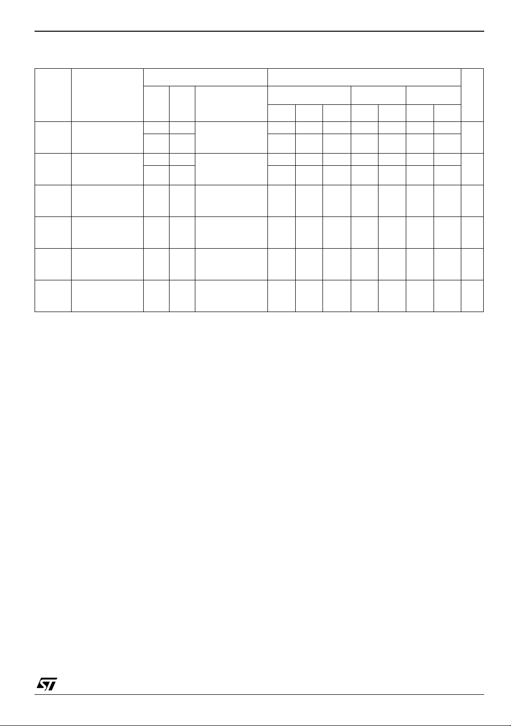
Table 8: Dynamic Switching Characteristics
Test Condition Value
Symbol Parameter
V
OLPA
Dynamic Low
Level Quiet
Output (note 1, 2)
V
OLPB
Dynamic Low
Level Quiet
Output (note 1, 2)
IHDA
Dynamic High
Voltage Input
V
(note 1, 3)
V
ILDA
Dynamic Low
Voltage Input
(note 1, 3)
IHDB
Dynamic High
Voltage Input
V
(note 1, 3)
V
ILDB
Dynamic Low
Voltage Input
(note 1, 3)
V
V
CCA
CCB
(V)
(V)
5.0 3.3 1.0 1.5
5.0 3.3 -1.2 -0.6
5.0 3.3 0.8 1.2
5.0 3.3 -0.8 -0.5
5.0 3.3 2 V
5.0 3.3 0.8 V
5.0 3.3 2 V
5.0 3.3 0.8 V
74LVXC4245
= 25 °C
T
A
Min. Typ. Max. Min. Max. Min. Max.
-40 to 85 °C -55 to 125°C
Unit
V
V
1) Worst case package
2) Max number of outp ut defined as (n). Data inputs are driven 0V to 3. 3V, (n-1) ou tp uts switchi ng and one outpu t at GND
3) Max number of data in puts (n) switching. (n-1) switching 0V to 3.3V . I nputs under tes t switching : 3V to threshol d (V
(V
) f = 1MHz
IHD
ILD
). 0V to threshold
5/14
 Loading...