

74LVX373
LOW VOLTAGE CMOS OCTAL D-TYPE LATCH
(3-STATE NON INV.) WITH 5V TOLERANT INPUTS
■ HIGH SPEED:
t
=5.8ns (TY P.) at VCC = 3.3V
PD
■ 5V TOLERANT INPUTS
■ POWER-DOWN PROTECTION ON INPUTS
■ INPUT VOLTAGE LEVEL:
V
= 0.8V, VIH = 2V at VCC =3V
IL
■ LOW POWER DISSIPATION:
I
= 4 µA (MAX.) at TA=25°C
CC
■ LOW NOISE:
V
= 0.3V (TYP.) at VCC =3.3V
OLP
■ SYMMETRICAL OUTPUT IMPEDANCE:
|I
| = IOL = 4 mA (MIN) at VCC =3V
OH
■ BALANCED PROPAGATION DELAYS:
t
≅ t
PLH
PHL
■ OPERATING VOLTAGE RANGE:
V
(OPR) = 2V to 3.6V (1.2V Data Retention)
CC
■ PIN AND FUNCTION COMPATIBLE WITH
74 SERIES 373
■ IMPROVED LATCH-UP IMMUNITY
DESCRIPTION
The 74LVX373 is a low voltage CMOS OCTAL
D-TYPE LATCH with 3 STATE OUTPUT NON
INVERTING fabricated with sub-micron silicon
gate and double-layer metal wiring C
2
MOS
technology. It is ideal for low power, battery
operated and low noise 3.3V applications.
This 8 bit D-Type latch is controlled by a latch
enable input (LE) and an output enable input (OE
).
While the LE in put is held at a high level, the Q
outpu ts w ill f o llow t h e d ata in put precis ely .
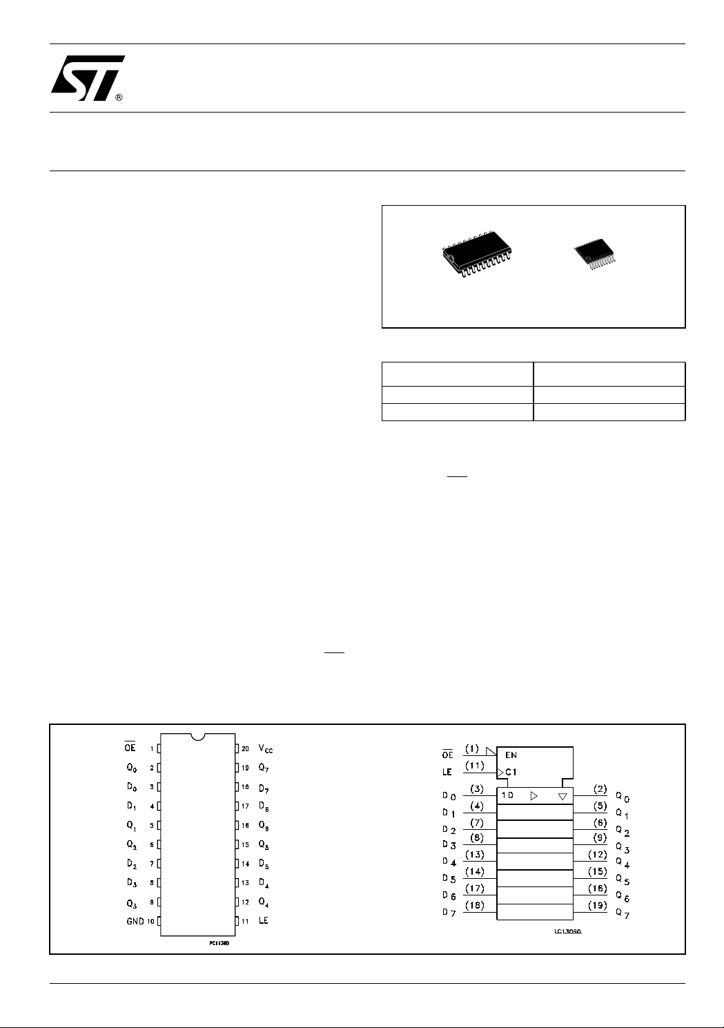
Figure 1: Pin C onnection And IEC Logic Symbol s
TSSOPSOP
Table 1: Order Codes
PACKAGE T & R
SOP 74LVX373MTR
TSSOP 74LVX373TTR
When the LE i s taken low, the Q outputs will be
latched precisely at the logic level of D input data.
While the (OE
) input is low, the 8 outputs will be in
a normal logic state (high or low logic level) and
while high level the outputs will be in a high
impedance state.
Power down protection is provided on all inputs
and 0 to 7V can be accepted on inputs with no
regard to the supply voltage.
This device can be used to interface 5V to 3V. It
combines high speed performance with the true
CMOS low power consumption.
All inputs and outputs are equipped with
protection circuits against static disc harge, giving
them 2KV ESD immunity and transient excess
voltage.
Rev. 4
1/13August 2004
74LVX373
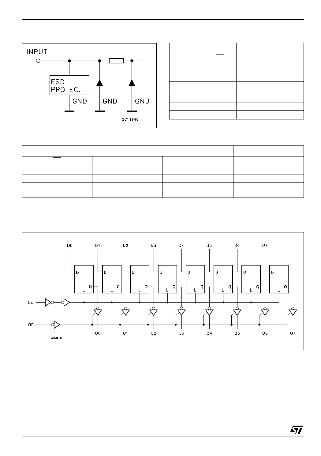
Figure 2: Input Equivalent Circuit Table 2: Pin Description
PIN N° SYMBOL NAME AND FUNCTION
Table 3: Truth Table
1OE
3, 4, 7, 8, 13,
D0 to D7 Data Inputs
14, 17, 18
2, 5, 6, 9, 12,
Q0 to Q7 3-State Outputs
15, 16,19
11 LE Latch Enable Input
10 GND Ground (0V)
20 V
CC
INPUTS OUTPUT
3 State Output Enable
Input (Active LOW)
Positive Supply Voltage
OE
LE D Q
HXXZ
LLXNO CHANGE*
LHLL
LHHH
X : Don’t Care
Z : High Impedance
* : Q Outputs are Latched at the time when the LE INPUT is taken low logic level
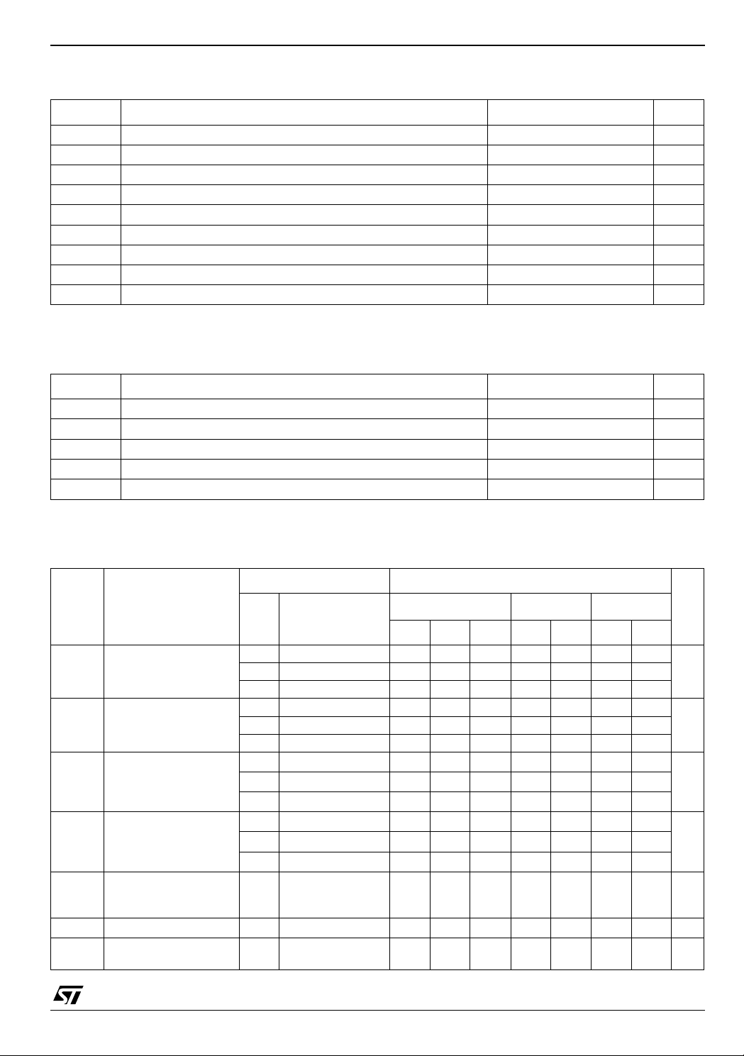
Figure 3: Logic Diagram
This logi c di agram has not be used to est i m ate propagation delays
2/13
74LVX373
Table 4: Absolute Maximum Ratings
Symbol Parameter Value Unit
V
V
V
I
I
OK
I
or I
I
CC
T
T
Absolute Maximum Ratings are those values beyond which damage to the device may occur. Functional operation under these conditions is
not implied
Table 5: Recommended Operating Conditions
Symbol Parameter Value Unit
V
V
V
T
dt/dv
1) Truth T abl e guarante ed: 1.2V to 3.6V
from 0.8V to 2.0V
2) V
IN
Table 6: DC Specifications
Supply Voltage
CC
DC Input Voltage
I
DC Output Voltage -0.5 to VCC + 0.5
O
DC Input Diode Current
IK
DC Output Diode Current
DC Output Current
O
DC VCC or Ground Current
GND
Storage Temperature
stg
Lead Temperature (10 sec)
L
Supply Voltage (note 1)
CC
Input Voltage
I
Output Voltage 0 to V
O
Operating Temperature
op
Input Rise and Fall Time (note 2) (V
CC
= 3V)
-0.5 to +7.0 V
-0.5 to +7.0 V
- 20 mA
± 20 mA
± 25 mA
± 50 mA
-65 to +150 °C
300 °C
2 to 3.6 V
0 to 5.5 V
CC
-55 to 125 °C
0 to 100 ns/V
V
V
Symbol Parameter
V
High Level Input
IH
Voltage
V
Low Level Input
IL
Voltage
V
High Level Output
OH
Voltage
V
Low Level Output
OL
Voltage
High Impedance
I
OZ
Output Leakage
Current
Input Leakage Current
I
I
Quiescent Supply
I
CC
Current
Test Condition Value
V
(V)
CC
T
A
Min. Typ. Max. Min. Max. Min. Max.
-40 to 85°C -55 to 125°C
= 25°C
2.0 1.5 1.5 1.5
2.0 2.0 2.0
3.6
2.4 2.4 2.4
2.0 0.5 0.5 0.5
3.6 0.8 0.8 0.8
=-50 µA
2.0
3.0
2.0
3.0
3.6
3.6
3.6
V
VO = VCC or GND
VI = 5V or GND
= VCC or GND
V
I
I
O
=-50 µA
I
O
=-4 mA
I
O
IO=50 µA
=50 µA
I
O
=4 mA
I
O
= VIH or V
I
1.9 2.0 1.9 1.9
2.9 3.0 2.9 2.9
2.58 2.48 2.4
0.0 0.1 0.1 0.1
0.0 0.1 0.1 0.1
0.36 0.44 0.55
IL
±0.25 ± 2.5 ± 5 µA
± 0.1 ± 1 ± 1 µA
44040µA
Unit
V3.0
V3.0 0.8 0.8 0.8
V3.0
V3.0
3/13
74LVX373
Table 7: Dynamic Switching Characteristics
Test Condition Value
= 25°C
Symbol Parameter
V
V
Dynamic Low
OLP
Voltage Quiet
OLV
Output (note 1, 2)
V
CC
(V)
3.3
T
A
Min. Typ. Max. Min. Max. Min. Max.
0.3 0.8
-0.8 -0.3
Dynamic High
V
IHD
Voltage Input
3.3 2.0
= 50 pF
C
L
(note 1, 3)
Dynamic Low
V
ILD
Voltage Input
3.3 0.8
(note 1, 3)
1) Worst case package.
2) Max number of outp ut s defined as (n). Data inp ut s are driven 0V to 3.3V, (n-1) outputs switc hi ng and one out put at GND.
3) Max number of data inputs (n) switching. (n-1) switching 0V to 3.3V. Inputs under test switching: 3.3V to threshold (V
(V
), f=1MHz.
IHD
Table 8: AC Electrical Characteristics (Input tr = tf = 3ns)
Test Condition Value
-40 to 85°C -55 to 125°C
ILD
Unit
V
), 0V to thresho l d
Symbol Parameter
t
Propagation Delay
PLH
PHL
PLH
PHL
PZL
PZH
PLZ
PHZ
t
W
t
S
t
h
Time
LE to Q
Propagation Delay
Time
D to Q
Output Enable
Time
Output Disable
Time
LE pulse Width,
HIGH
Setup Time D to LE
HIGH or LOW
Hold Time D to LE
HIGH or LOW
Output to Output
Skew Time (note
1,2)
t
t
t
t
t
t
t
t
OSLH
t
OSHL
V
(V)
CC
C
(pF)
T
L
A
Min. Typ. Max. Min. Max. Min. Max.
-40 to 85°C -55 to 125°C
= 25°C
2.7 15 7.5 14.5 1.0 17.5 1.0 18.5
2.7 50 10.0 18.0 1.0 21.0 1.0 22.0
(*)
3.3
3.3
15 6.8 10.3 1.0 12.0 1.0 13.0
(*)
50 9.3 13.8 1.0 15.5 1.0 16.5
2.7 15 7.7 15.0 1.0 18.5 1.0 19.5
2.7 50 10.2 18.5 1.0 22.0 1.0 23.0
(*)
3.3
3.3
15 5.8 9.7 1.0 11.5 1.0 12.5
(*)
50 8.5 13.2 1.0 15.0 1.0 16.0
2.7 15 7.7 15.0 1.0 18.5 1.0 19.5
2.7 50 10.2 18.5 1.0 22.0 1.0 23.0
(*)
3.3
3.3
15 6.0 9.7 1.0 11.5 1.0 12.5
(*)
50 8.5 13.2 1.0 15.0 1.0 16.0
2.7 50 9.8 18.0 1.0 21.0 1.0 22.0
(*)
3.3
50 8.2 12.8 1.0 14.5 1.0 15.5
2.7 50 6.5 7.5 7.5
(*)
3.3
50 5.0 5.0 5.0
2.7 50 6.0 6.0 6.0
(*)
3.3
50 4.0 4.0 4.0
2.7 50 1.0 1.0 1.0
(*)
3.3
50 1.0 1.0 1.0
2.7 50 0.5 1.0 1.5 1.5
(*)
3.3
50 0.5 1.0 1.5 1.5
Unit
ns
ns
ns
ns
ns
ns
ns
ns
1) Skew is defined as the absolute value of the difference between the actual propagation delay for any two outputs of the same device switching in the sa m e di rection, ei ther HIGH or LOW
2) Param eter guaran teed by design
(*) Voltage range is 3.3V ±
0.3V
4/13
 Loading...