

74LVX3245
OCTAL DUAL SUPPLY BUS TRANSCEIVER
■ HIGH SPEED:
t
= 8ns (MAX.) at TA=25°C
PD
V
= 3.3V, V
CCA
■ LOW POWER DISSIPATION:
I
= I
CCA
■ LOW NOISE: V
■ SYMMETRICAL OUTPUT IMPEDANCE:
|I
| = IOL = 24mA (MIN)
OH
■ BALANCED PROPAGATION DELAYS:
t
≅ t
PLH
■ OPERATING VOLT AG E R AN GE:
V
CCA
V
CCB
= 5µA(MAX.) at TA=25°C
CCB
PHL
(OPR) = 2.7V to 3.6V (1.2V Data Retention)
(OPR) = 4.5V to 5.5V (1.2V Data Retention)
= 5.0V
CCB
=0.3V (TYP.) at VCC =3.3V
OLP
PIN AND FUNCTION COMPATIBLE WITH
74 SERIES 3245
■ IMPROVED LATCH-UP I MMUN ITY
DESCRIPTION
The 74LVX3245 is a dual supply low voltage
CMOS OCTAL BUS TRANSCEIVER fabricated
with sub-micron silicon gate and double-layer
metal wiring C
2
MOS technology. Designed for use
as an interface between a 5V bus and a 3. 3V bus
in a mixed 5V/3.3V supply systems, it achieves
high speed operation while maintaining the CMOS
low power dissipation.
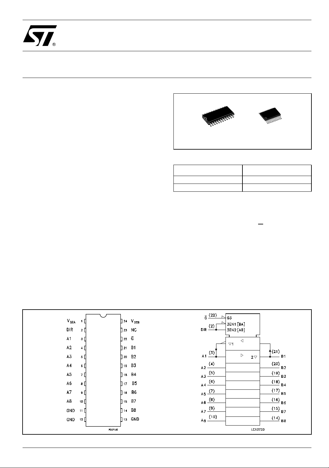
TSSOPSOP
Table 1: Order Codes
PACKAGE T & R
SOP 74LVX3245MTR
TSSOP 74LVX3245TTR
This IC is intended for two-way asynchronous
communication between data buses and the
direction of data transmission is determined by
DIR input. The enable input G
can be used to
disable the device so that the buses are effectively
isolated.
The A-port interfaces with the 3V bus, the B-port
with the 5V bus.
All inputs are equipped with protection circuits
against static discharge, giving them 2KV ESD
immunity and transient excess voltage.
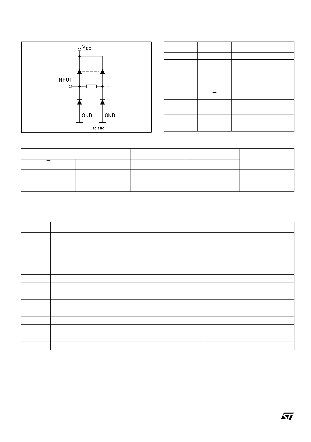
Figure 1: Pin Connection And IEC Logic Symbols
Rev. 4
1/13August 2004
74LVX3245
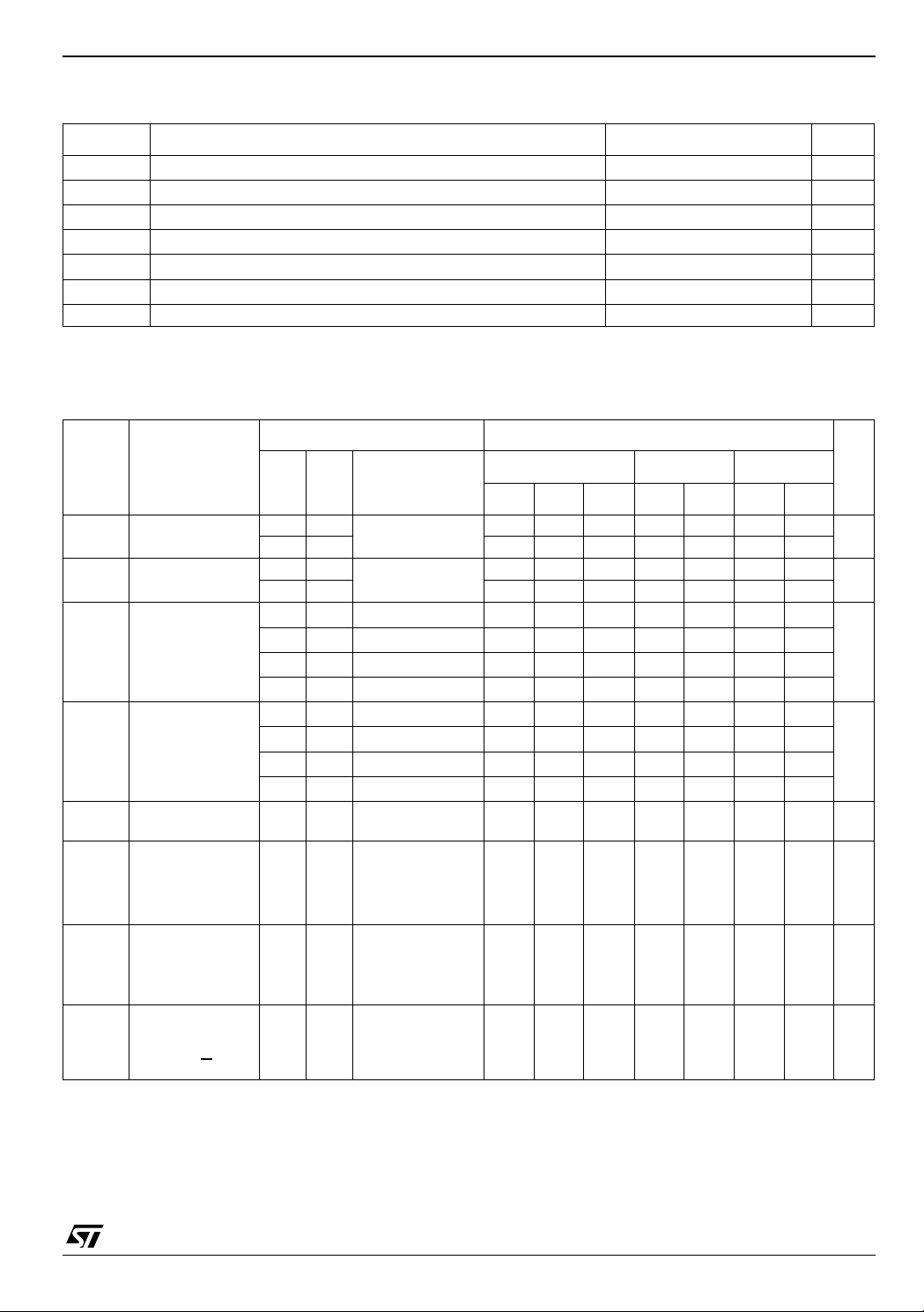
Figure 2: Input And Output Equivalent Circuit Table 2: Pin Description
PIN N° SYMBOL NAME QND FUNCTION
2 DIR Directional Control
3, 4, 5, 6, 7,
8, 9, 10
21, 20, 19,
18, 17, 16,
15, 14
22 G
11, 12, 13 GND Ground (0V)
23 NC Not Connected
1V
24 V
Table 3: Truth Tab l e
A1 to A8 Data Inputs/Outputs
B1 to B8 Data Inputs/Outputs
Output Enable Input
CCA
CCB
Positive Supply Voltage
Positive Supply Voltage
INPUTS FUNCTION
OUTPUT
G
DIR A BUS B BUS
L L OUTPUT INPUT A = B
L H INPUT OUTPUT B = A
HXZZZ
X : Don’t Care
Z : High Impedance
Table 4: Absolute Maximum Ratings
Symbol Parameter Value Unit
V
CCA
V
CCB
V
V
I/OA
V
I/OB
I
I
OK
I
OA
I
OB
I
CCA
I
CCB
P
T
T
Absolute Maximum Ratings are those values beyond which damage to the device may occur. Functional operation under these conditions is
not implied
Supply Voltage
Supply Voltage
DC Input Voltage -0.5 to V
I
DC I/O Voltage -0.5 to V
DC I/O Voltage -0.5 to V
DC Input Diode Current
IK
DC Output Diode Current
DC Output Current
DC Output Current
DC VCC or Ground Current
DC VCC or Ground Current
Power Dissipation
d
Storage Temperature
stg
Lead Temperature (10 sec)
L
-0.5 to +7.0 V
-0.5 to +7.0 V
+ 0.5
CCA
+ 0.5
CCA
+ 0.5
CCB
± 20 mA
± 50 mA
± 50 mA
± 50 mA
± 200 mA
± 100 mA
180 mW
-65 to +150 °C
300 °C
V
V
V
2/13
74LVX3245
Table 5: Recommended Operating Conditions
Symbol Parameter Value Unit
V
CCA
V
CCB
V
V
I/OA
V
I/OB
T
dt/dv Input Rise and Fall Time (note 2) 0 to 10 ns/V
Supply Voltage (note 1)
Supply Voltage (note 1)
Input Voltage 0 to V
I
I/O Voltage 0 to V
I/O Voltage 0 to V
Operating Temperature
op
2.7 to 3.6 V
4.5 to 5.5 V
CCA
CCA
CCB
-55 to 125 °C
V
V
V
1) VIN from 30 % t o 70% of V
2) V
= 2.7 to 3.6V; V
CCA
CC
= 4.5 to 5.5V;
CCB
Table 6: DC Specifications For V
Test Condition Value
Symbol Parameter
V
High Level Input
IHA
Voltage
V
Low Level Input
ILA
Voltage
V
V
High Level
OHA
Output Voltage
Low Level Output
OLA
Voltage
Input Leakage
I
IA
Current
High Impedance
I
OZA
Output Leakage
Current
I
∆I
Qui esce nt Su pply
CCtA
Current
Maximum
CCtA
Qui esce nt Su pply
Current / Input
(An, DIR, G
V
V
CCA
(V)
(V)
3.6 5.0 2.0 2.0 2.0
2.7 5.0 2.0 2.0 2.0
3.6 5.0 0.8 0.8 0.8
2.7 5.0 0.8 0.8 0.8
3.0 4.5
3.0 4.5
2.7 4.5
2.7 4.5
3.0 4.5
3.0 4.5
2.7 4.5
2.7 4.5
3.6 5.5
3.6 5.5 VIA = V
3.6 5.5 VIA = V
3.6 5.5 V
)
CCB
CCA
IO=-100 µA
= VCC or GND
V
I
VIB = V
V
I/OA
VIB = V
= V
IA
V
I
=-24 mA
O
=-12 mA
I
O
=-24 mA
I
O
IO=100 µA
I
=24 mA
O
I
=12 mA
O
=24 mA
I
O
or V
IHA
or V
IHB
= V
CCA
GND
CCA
GND
CCB
GND
- 0.6V
CCA
= V
IB
CCB
GND
= 25 °C
T
A
-40 to 85 °C -55 to 125°C
Min. Typ. Max. Min. Max. Min. Max.
2.9 2.99 2.9 2.9
2.35 2.65 2.25 2.25
2.3 2.5 2.2 2.2
2.1 2.3 2.0 2.0
0.002 0.1 0.1 0.1
0.21 0.36 0.44 0.44
0.11 0.36 0.44 0.44
0.22 0.42 0.5 0.5
± 0.1 ± 1 ± 1 µA
ILA
ILB
± 0.5 ± 5 ± 5 µA
or
or
55050µA
or
0.35 0.5 0.5 mA
or
Unit
V
V
V
V
3/13
74LVX3245
Table 7: DC Specifications For V
Test Condition Value
Symbol Parameter
V
High Level Input
IHB
Voltage
V
Low Level Input
ILB
Voltage
V
V
High Level
OHB
Output Voltage
Low Level Output
OLB
Voltage
Input Leakage
I
IB
Current
High Impedance
I
OZB
Output Leakage
Current
I
∆I
Qui esce nt Su pply
CCtB
Current
Maximum
CCtB
Qui esce nt Su pply
Current / Input
V
V
CCA
(V)
(V)
3.3 4.5 2.0 2.0 2.0
3.3 5.5 2.0 2.0 2.0
3.3 4.5 0.8 0.8 0.8
3.3 5.5 0.8 0.8 0.8
3.0 4.5
3.3 4.5
3.0 4.5
3.3 4.5
3.6 5.5
3.6 5.5 VIA = V
3.6 5.5 VIA = V
3.6 5.5 VIA = V
CCB
CCB
I
O
I
O
IO=100 µA
I
O
= V
V
I
V
I/Ob
V
IB
VIB = V
=-100 µA
=-24 mA
=24 mA
or GND
CCA
or V
IHA
= V
CCb
GND
CCA
GND
= V
CCB
GND
CCA
GND
- 2.1V
CCB
= 25 °C
T
A
-40 to 85 °C -55 to 125°C
Min. Typ. Max. Min. Max. Min. Max.
4.4 4.5 4.4 4.4
3.86 4.25 3.75 3.75
0.002 0.1 0.1 0.1
0.18 0.36 0.44 0.44
± 0.1 ± 1 ± 1 µA
ILA
± 0.5 ± 5 ± 5 µA
or
or
88080µA
or
or
1.35 1.5 1.5 mA
Unit
V
V
V
V
Table 8: Dynamic Switching Characteristics
Test Condition Value
= 25 °C
Symbol Parameter
V
OLPA
Dynamic Low
Level Quiet
Output (note 1, 2)
OLPB
Dynamic Low
Level Quiet
V
Output (note 1, 2)
V
IHDA
Dynamic High
Voltage Input
V
V
CCA
CCB
(V)
(V)
3.3 5.0 1.0 1.5
3.3 5.0 -1.2 -0.6
3.3 5.0 0.8 1.2
3.3 5.0 -0.8 -0.5
3.3 5.0 2 V
(note 1, 3)
ILDA
Dynamic Low
Voltage Input
3.3 5.0 0.8 V
V
(note 1, 3)
V
IHDB
Dynamic High
Voltage Input
3.3 5.0 2 V
(note 1, 3)
V
ILDB
Dynamic Low
Voltage Input
3.3 5.0 0.8 V
(note 1, 3)
1) Worst case package
2) Max number of outp ut defined as (n). Data inputs are driven 0V to 3. 3V, (n-1) ou tp uts switchi ng and one outpu t at GND
3) Max number of data in puts (n) switching. (n-1) switching 0V to 3.3V . I nputs under tes t switching : 3V to threshol d (V
) f = 1MHz
(V
IHD
T
A
-40 to 85 °C -55 to 125°C
Min. Typ. Max. Min. Max. Min. Max.
ILD
Unit
V
V
). 0V to threshold
4/13
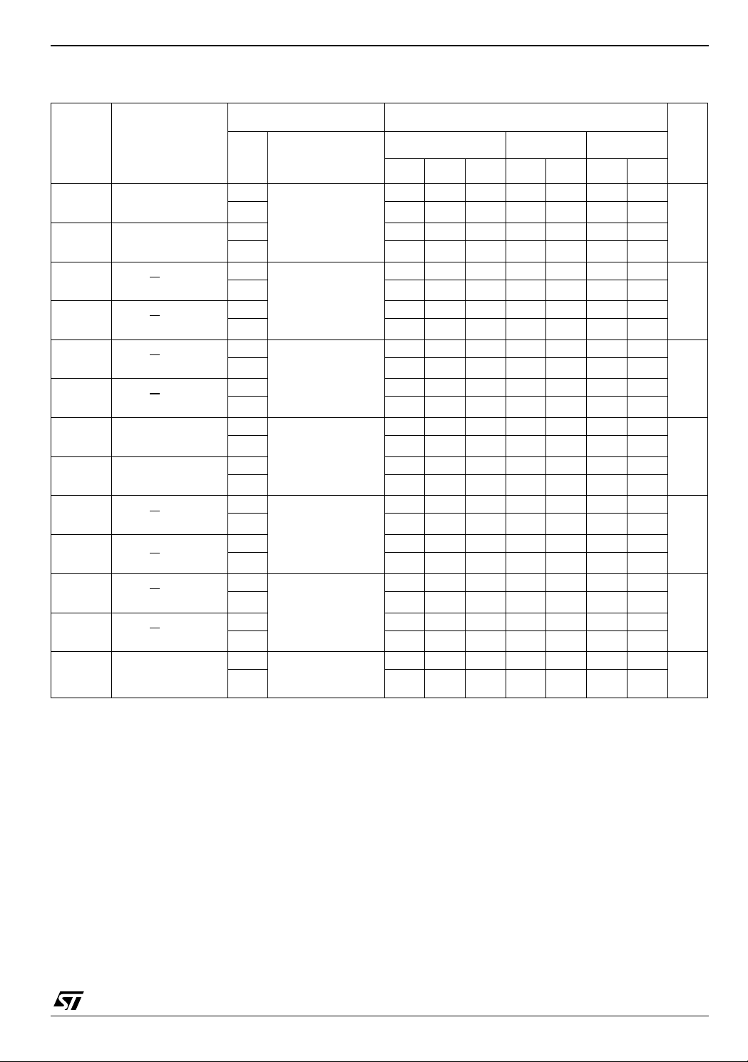
Table 9: AC Electrical Characteristics (CL = 50pF, Input tr = tf = 3ns)
74LVX3245
Symbol Parameter
t
t
t
t
t
t
t
t
Propagation Delay
PLH
Time (An to Bn)
Propagation Delay
PHL
Time (An to Bn)
Output Enable
PZL
Time (G
Output Enable
PZH
Time (G
Output Disable
PLZ
Time (G
Output Disable
PHZ
Time (G
Propagation Delay
PLH
Time (Bn to An)
PHL
Propagation Delay
to Bn)
to Bn)
to Bn)
to Bn)
Time (Bn to An)
t
t
t
t
t
OSLH
t
OSHL
Output Enable
PZL
Time (G
PZH
Output Enable
Time (G
Output Disable
PLZ
Time (G
Output Disable
PHZ
Time (G
Output To Output
Skew Time (note1,
2)
to An)
to An)
to An)
to An)
Test Condition
V
CCA
(V)
= 25°C
T
A
Min. Typ. Max. Min. Max. Min. Max.
(3)
Value
-40 to 85°C -55 to 125°C
2.7 1.0 9.0 1.0 10.0
3.0
(*)
1.0 5.4 8.0 1.0 8.5 1.0 9.5
2.7 1.0 8.5 1.0 9.5
3.0
(*)
1.0 5.6 7.5 1.0 8.0 1.0 9.5
2.7 1.0 9.0 1.0 10.0
3.0
(*)
1.0 4.8 8.0 1.0 8.5 1.0 9.5
2.7 1.0 9.5 1.0 10.5
3.0
(*)
1.0 6.3 8.5 1.0 9.0 1.0 10.0
2.7 1.0 8.5 1.0 9.5
3.0
(*)
1.0 5.3 7.5 1.0 8.5 1.0 9.5
2.7 1.0 8.0 1.0 9.0
3.0
(*)
1.0 4.2 7.0 1.0 7.5 1.0 8.5
2.7 1.0 8.5 1.0 9.5
3.0
(*)
1.0 5.1 7.5 1.0 8.0 1.0 8.5
2.7 1.0 8.5 1.0 9.0
3.0
(*)
1.0 5.7 7.5 1.0 8.0 1.0 8.5
2.7 1.0 9.5 1.0 10.0
3.0
(*)
1.0 6.3 8.5 1.0 9.0 1.0 9.5
2.7 1.0 10.0 1.0 10.5
3.0
(*)
1.0 6.8 9.0 1.0 9.5 1.0 10.0
2.7 1.0 9.0 1.0 9.5
3.0
(*)
1.0 5.3 8.0 1.0 8.5 1.0 9.0
2.7 1.0 7.5 1.0 8.0
3.0
(*)
1.0 3.7 6.5 1.0 7.0 1.0 8.0
2.7 0.5 1.0 1.5 1.5
3.0
(*)
0.5 1.0 1.5 1.5
Unit
ns
ns
ns
ns
ns
ns
ns
1) Skew is defined as the absolute value of the difference between the actual propagation delay for any two outputs of the same device switch-
ing in the sa m e di rection, ei ther HIGH or LOW
2) Param eter guaran teed by design
3) Typical values at V
(*) Voltage range is 3.0V ±
CCA
= 3.3V, V
0.3V
CCB
= 5.0V
5/13
74LVX3245
Table 10: Capacitive Characteristics
Test Condition Value
Symbol Parameter
C
Input
IN
Capacitance
C
Input/Output
I/O
Capacitance
C
Dynamic Low
PD
Level Quiet
Output (note 1)
A to B
Dynamic Low
C
PD
Level Quiet
Output (note 1)
B to A
V
V
CCA
CCB
(V)
(V)
open open 4.5 V
3.3 5.0 10 V
3.3 5.0 55 V
3.3 5.0 40 V
= 25 °C
T
A
-40 to 85 °C -55 to 125°C
Min. Typ. Max. Min. Max. Min. Max.
Unit
1) CPD is defined as the value of the IC’s internal equivalent capacitance which is calculated from the operating current consumption without
load. (R efer to Test Circuit). Average curre nt can be obta i ned by the following equa t i on. I
= CPD x VCC x fIN + ICC/8 (per circuit)
CC(opr)
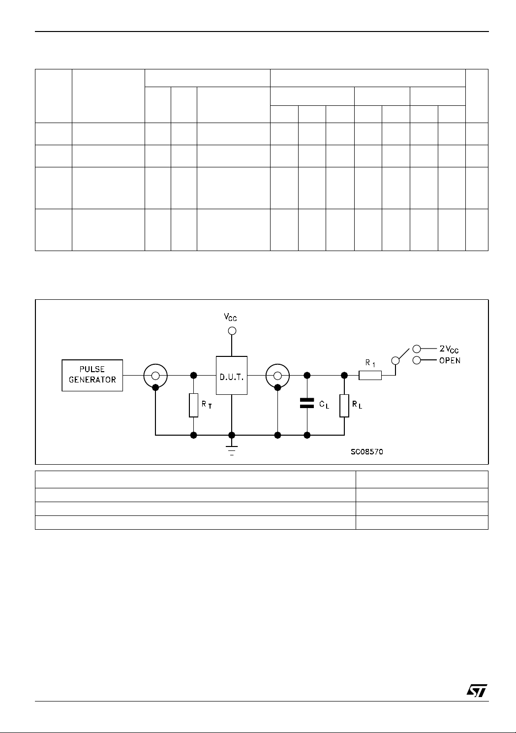
Figure 3: Test Circuit
TEST SWITCH
, t
t
PLH
PHL
, t
t
PZL
PLZ
t
, t
PZH
PHZ
CL = 50pF or equivalent (includes jig and p robe capacit ance)
R
= R1 = 500Ω or equivalent
L
R
= Z
of pulse generator (typically 50Ω)
T
OUT
Open
2V
CC
Open
6/13
74LVX3245
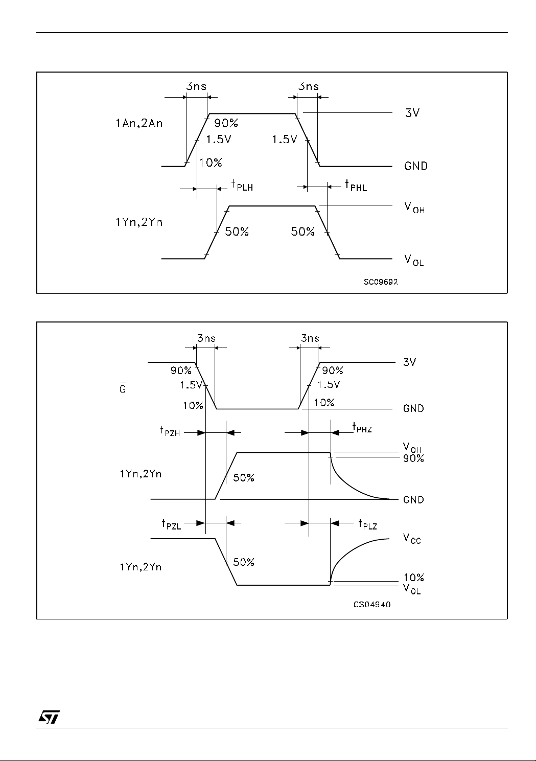
Figure 4: Waveform - Propagation Delays (f=1MHz; 50% duty cycle)
Figure 5: Waveform - Output Enable And Disable Time (f=1MHz; 50% duty cycle)
7/13

74LVX3245
SO-24 MECHANICAL DATA
DIM.
A 2.35 2.65 0.093 0.104
A1 0.1 0.30 0.004 0.012
B 0.33 0.51 0.013 0.020
C 0.23 0.32 0.009 0.013
D 15.20 15.60 0.598 0.614
E 7.4 7.6 0.291 0.299
e 1.27 0.050
H 10.00 10.65 0.394 0.419
h 0.25 0.75 0.010 0.030
L 0.4 1.27 0.016 0.050
k0° 8° 0° 8°
ddd 0.100 0.004
MIN. TYP MAX. MIN. TYP. MAX.
mm. inch
8/13
0070769C

74LVX3245
TSSOP24 MECHANICAL DATA
mm. inch
DIM.
MIN. TYP MAX. MIN. TYP. MAX.
A 1.1 0.043
A1 0.05 0.15 0.002 0.006
A2 0.9 0.035
b 0.19 0.30 0.0075 0.0118
c 0.09 0.20 0.0035 0.0079
D 7.7 7.9 0.303 0.311
E 4.3 4.5 0.169 0.177
e 0.65 BSC 0.0256 BSC
H 6.25 6.5 0.246 0.256
K0° 8° 0° 8°
L 0.50 0.70 0.020 0.028
A2
A
A1
b
e
D
K
c
E
L
H
PIN 1 IDENTIFICATION
1
7047476B
9/13

74LVX3245
Tape & Reel SO-24 MECHANICAL DATA
mm. inch
DIM.
MIN. TYP MAX. MIN. TYP. MAX.
A 330 12.992
C 12.8 13.2 0.504 0.519
D 20.2 0.795
N 60 2.362
T 30.4 1.197
Ao 10.8 11.0 0.425 0.433
Bo 15.7 15.9 0.618 0.626
Ko 2.9 3.1 0.114 0.122
Po 3.9 4.1 0.153 0.161
P 11.9 12.1 0.468 0.476
10/13

74LVX3245
Tape & Reel TSSOP24 MECHANICAL DATA
mm. inch
DIM.
MIN. TYP MAX. MIN. TYP. MAX.
A 330 12.992
C 12.8 13.2 0.504 0.519
D 20.2 0.795
N 60 2.362
T 22.4 0.882
Ao 6.8 7 0.268 0.276
Bo 8.2 8.4 0.323 0.331
Ko 1.7 1.9 0.067 0.075
Po 3.9 4.1 0.153 0.161
P 11.9 12.1 0.468 0.476
11/13
74LVX3245
Table 11: Revision History
Date Revision D escrip tion of Change s
27-Aug-2004 4 Ordering Codes Revision - pag. 1.
12/13

74LVX3245
Information furnished is believed to be accurate and reliable. However, STMicroelectronics assumes no responsibility for the consequences
of use of s uch inf ormati on nor for a ny infr ing eme nt o f p atent s or o ther ri ghts of third parties wh ich m ay res ul t from i ts use. N o lic ense i s gran ted
by implication or otherwise under any patent or patent rights of STMicroelectronics. Specifications mentioned in this publication are subject
to change without notice. This publication supersedes and replaces all information previously supplied. STMicroelectronics products are not
authorized for use as critical components in life support devices or systems without express written approval of STMicroelectronics.
The ST logo is a registered trademark of STMicroelectronics
All other names are the property of their respective owners
© 2004 STMicroelectronics - All Rights Reserved
STMicroelectronics group of companies
Australia - Belgium - Brazil - Canada - China - Czech Republic - Finland - France - Germany - Hong Kong - India - Israel - Italy - Japan -
Malaysia - Malta - Morocco - Singapore - Spain - Sweden - Switzerland - United Kingdom - United States of America
www.st.com
13/13
 Loading...