

74LVX20
Obsolete Product(s) - Obsolete Product(s)
LOW VOLTAGE CMOS DUAL 4-INPUT NAND GATE
WITH 5V TOLERANT INPUTS
■ HIGH SPEED:
t
= 4.1ns (TYP.) at V
PD
■ 5V TOLERANT INPUTS
■ INPUT VOLTAGE LEVEL:
V
=0.8V , VIH=2V at VCC=3V
IL
■ LOW POWER DISSIPATION:
I
= 2 µA (MAX.) at TA=25°C
CC
■ LOW NOISE:
V
= 0.3V (TYP.) at VCC = 3.3V
OLP
■ SYMMETRICAL OUTPUT IMPEDANCE:
|I
| = IOL = 4mA (MIN)
OH
■ BALANCED PROPAGATION DELAYS:
t
≅ t
PLH
PHL
■ OPERATING VOLTAGE RANGE:
V
(OPR) = 2V to 3.6V (1.2V Data Retention)
CC
■ PIN AND FUNCTION COMPATIBLE WITH
CC
= 3.3V
74 SERIES 20
■ IMPROVED LATCH-UP IMMUN ITY
■ POWER DOWN PROTECTION ON INPUTS
DESCRIPTION
The 74LVX20 is a low voltage CMOS DUAL
4-INPUT NAND GATE fabricated with sub-micron
silicon gate and double-layer metal wiring C
2
MOS
technology. It is ideal for low power, battery
operated and low noise 3.3V applications.
TSSOPSOP
Table 1: Order Codes
PACKAGE T & R
SOP 74LVX20MTR
TSSOP 74LVX20TTR
The internal circuit is composed of 3 stages
including buffer ou tput, whi ch provid es hig h no ise
immunity and stable output.
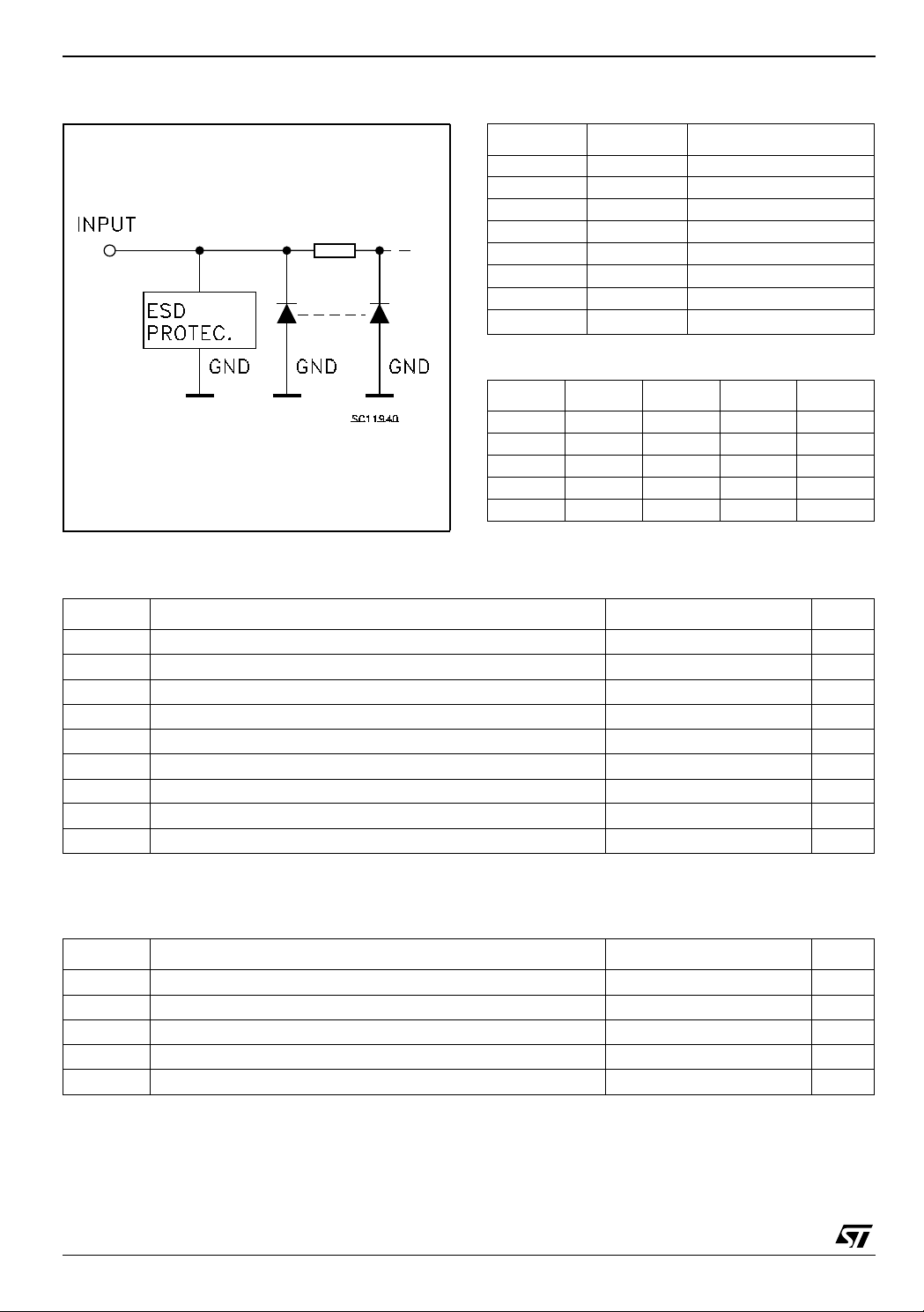
Power down protection is provided on all inputs
and 0 to 7V can be accepted on inputs with no
regard to the supply voltage.
This device can be used to interface 5V to 3V
system. It combines high speed performance with
the true CMOS low power consumption.
All inputs and outputs are equipped with
protection circuits against static disc harge, giving
them 2KV ESD immunity and transient excess
voltage.
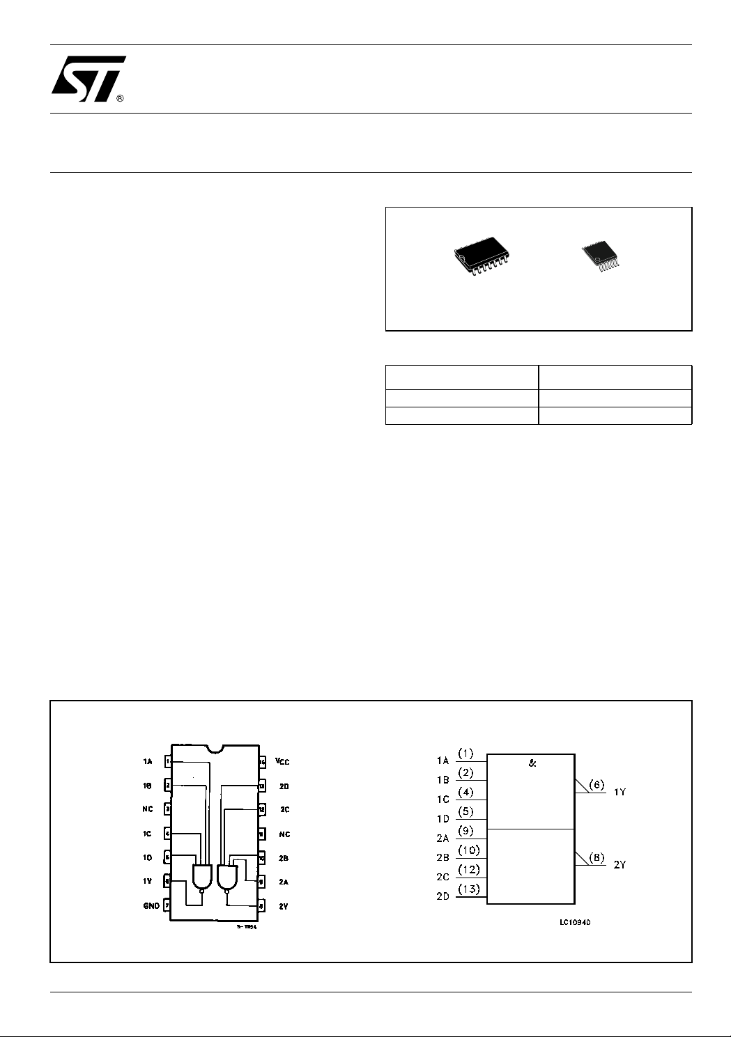
Figure 1: Pin Connection An d I E C Logic Symbols
Rev. 3
1/11August 2004
Obsolete Product(s) - Obsolete Product(s)
74LVX20
Figure 2: Input Equivalent Circuit Table 2: Pin Description
PIN N° SYMBOL NAME AND FUNCTION
1, 9 1A to 2A Data Inputs
2, 10 1B to 2B Data Inputs
3, 11 N.C. Not Connected
4, 12 1C to 2C Data Inputs
5, 13 1D to 2D Data Inputs
6, 8 1Y to 2Y Data Outputs
7 GND Ground (0V)
14
Table 3: Truth Table
ABCDY
LXXXH
XLXXH
XXLXH
XXXLH
HHHHL
X : Don‘t Care
V
CC
Positive Supply Voltage
Table 4: Absolute Maximum Ratings
Symbol Parameter Value Unit
V
V
V
I
I
OK
I
or I
I
CC
T
T
Absolute Maximum Ratings are those values beyond which damage to the device may occur. Functional operation under these conditions is
not implied.
Supply Voltage
CC
DC Input Voltage
I
DC Output Voltage -0.5 to VCC + 0.5
O
DC Input Diode Current
IK
DC Output Diode Current
DC Output Current
O
DC VCC or Ground Current
GND
Storage Temperature
stg
Lead Temperature (10 sec)
L
-0.5 to +7.0 V
-0.5 to +7.0 V
V
- 20 mA
± 20 mA
± 25 mA
± 50 mA
-65 to +150 °C
300 °C
Table 5: Recommended Operating Conditions
Symbol Parameter Value Unit
V
V
V
T
dt/dv
1) Truth T abl e guarante ed: 1.2V to 3.6V
2) VIN from 0.8V to 2.0V
Supply Voltage (note 1)
CC
Input Voltage
I
Output Voltage 0 to V
O
Operating Temperature
op
Input Rise and Fall Time (note 2) (V
= 3.3V)
CC
2 to 3.6 V
0 to 5.5 V
CC
-55 to 125 °C
0 to 100 ns/V
V
2/11
Obsolete Product(s) - Obsolete Product(s)
Table 6: DC Specifications
Symbol Parameter
V
V
V
High Level Input
IH
Voltage
V
Low Level Input
IL
Voltage
High Level Output
OH
Voltage
Low Level Output
OL
Voltage
Input Leakage
I
I
Current
I
Quiescent Supply
CC
Current
Test Condition Value
V
(V)
CC
T
A
Min. Typ. Max. Min. Max. Min. Max.
-40 to 85°C -55 to 125°C
= 25°C
2.0 1.5 1.5 1.5
3.6 2.4 2.4 2.4
2.0 0.5 0.5 0.5
3.6 0.8 0.8 0.8
=-50 µA
2.0
3.0
2.0
3.0
3.6
3.6
I
O
=-50 µA
I
O
=-4 mA
I
O
IO=50 µA
I
=50 µA
O
=4 mA
I
O
= 5V or GND
V
I
V
= VCC or GND
I
1.9 2.0 1.9 1.9
2.9 3.0 2.9 2.9
2.58 2.48 2.4
0.0 0.1 0.1 0.1
0.0 0.1 0.1 0.1
0.36 0.44 0.55
± 0.1 ± 1 ± 1 µA
22020µA
74LVX20
Unit
V3.0 2.0 2.0 2.0
V3.0 0.8 0.8 0.8
V3.0
V3.0
Table 7: Dynamic Switching Characteristics
Test Condition Value
Symbol Parameter
V
V
V
Dynamic Low
OLP
Voltage Quiet
OLV
Output (note 1, 2)
Dynamic High
IHD
Voltage Input (note
V
CC
(V)
3.3
3.3 2
= 50 pF
C
L
T
A
Min. Typ. Max. Min. Max. Min. Max.
0.3 0.5
-0.5 -0.3
-40 to 85°C -55 to 125°C
Unit
V
= 25°C
1, 3)
V
Dynamic Low
ILD
Voltage Input (note
3.3 0.8
1, 3)
1) Worst case package.
2) Max number of outp ut s defined as (n). Data inp ut s are driven 0V to 3.3V, (n-1) outputs switc hi ng and one out put at GND.
3) Max number of data inputs (n) switching. (n-1) switching 0V to 3.3V. Inputs under test switching: 3.3V to threshold (V
(V
), f=1MHz.
IHD
), 0V to thresho l d
ILD
3/11
Obsolete Product(s) - Obsolete Product(s)
74LVX20
Table 8: AC Electrical Characteristics (Input tr = tf = 3ns)
Test Condition Value
= 25°C
Symbol Parameter
t
PLH tPHL
t
OSLH
t
OSHL
1) Skew is defined as the absolute value of the difference between the actual propagation delay for any two outputs of the same device switching in the sa m e di rection, ei ther HIGH or LOW
2) Param eter guaran teed by design
(*) Voltage range is 3.3V ±
Propagation Delay
Time
Output To Output
Skew Time (note1,
2)
0.3V
V
C
CC
(V)
L
(pF)
2.7 15 8.6 1.0 10.5 1.0 11.5
2.7 50 13.5 1.0 15.4 1.0 16.4
(*)
3.3
3.3
15 4.1 6.2 1.0 7.5 1.0 9.5
(*)
50 6.6 9.7 1.0 11.0 1.0 12.0
2.7 50 0.5 1.0 1.5 1.5
(*)
3.3
50
T
A
Min. Typ. Max. Min. Max. Min. Max.
0.5 1.0 1.5 1.5
Table 9: Capacitive Characteristics
Test Condition Value
= 25°C
Symbol Parameter
C
C
Input Capacitance
IN
Power Dissipation
PD
Capacitance
(note 1)
V
CC
(V)
3.3 4 10 10 10 pF
3.3 19 pF
T
A
Min. Typ. Max. Min. Max. Min. Max.
-40 to 85°C -55 to 125°C
-40 to 85°C -55 to 125°C
Unit
ns
ns
Unit
1) CPD is defined as the value of the IC’s internal equivalent capacitance which is calculated from the operating current consumption without
load. (Refer to Test Circuit). Average operating current can be obtained by the following equation. I
= CPD x VCC x fIN + ICC/2 (per gate)
CC(opr)
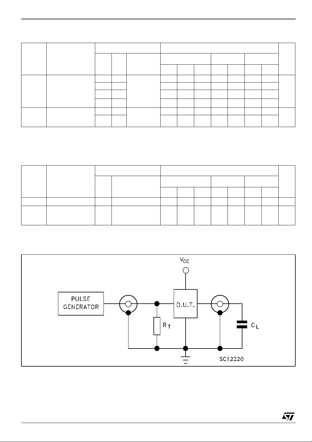
Figure 3: Test Circuit
CL =15/50pF or equivalent (i ncludes jig an d probe capac i tance)
R
= Z
of pulse generator (typically 50Ω)
T
OUT
4/11
 Loading...