

查询74LVQ74供应商
74LVQ74
DUAL D-TYPE FLIP FLOP WITH PRESET AND CLEAR
■ HIGHSPEED:
=250MHz(TYP.)at VCC=3.3V
f
MAX
■ COMPATIBLEWITHTTLOUTPUTS
■
LOW POWERDISSIPAT ION:
I
=2 µA (MAX.)at TA=25oC
CC
■ LOWNOISE:
=0.2V (TYP.)at VCC=3.3V
V
OLP
■ 75Ω TRANSMISSIONLINEDRIVING
CAPABILITY
■ SYMMETRICALOUTPUTIMPEDANCE:
|I
|=IOL=12mA (MIN)
OH
■
PCIBUSLEVELSGUARANTEEDAT24mA
■ BALANCEDPROPAGATIONDELAYS:
t
≅ t
PLH
PHL
■ OPERATINGVOLTAGERANGE:
V
(OPR)= 2V to 3.6V(1.2VDataRetention)
CC
■
PINANDFUNCTIONCOMPATIBLEWITH
74SERIES74
■ IMPROVEDLATCH-UP IMMUNITY
DESCRIPTION
The LVQ74 is a low voltage CMOS DUAL
D-TYPEFLIP FLOP WITH PRESETAND CLEAR
NON INVERTING fabricated with sub-micron
silicon gate and double-layermetal wiring C
2
MOS
technology.It is ideal for low power and low noise
(Micro Package)
3.3Vapplications.
A signal on the D INPUT is transferred to the Q
OUTPUT during the positive going transition of
the clock pulse.
CLEAR and PRESET are independent of the
clock and accomplished by a low setting on the
appropriateinput.
It has better speed performance at 3.3V than 5V
LSTTL family combined with the true CMOS low
powerconsumption.
All inputs and outputs are equipped with
protection circuits against static discharge, giving
them 2KV ESD immunity and transient excess
voltage.
M
(TSSOPPackage)
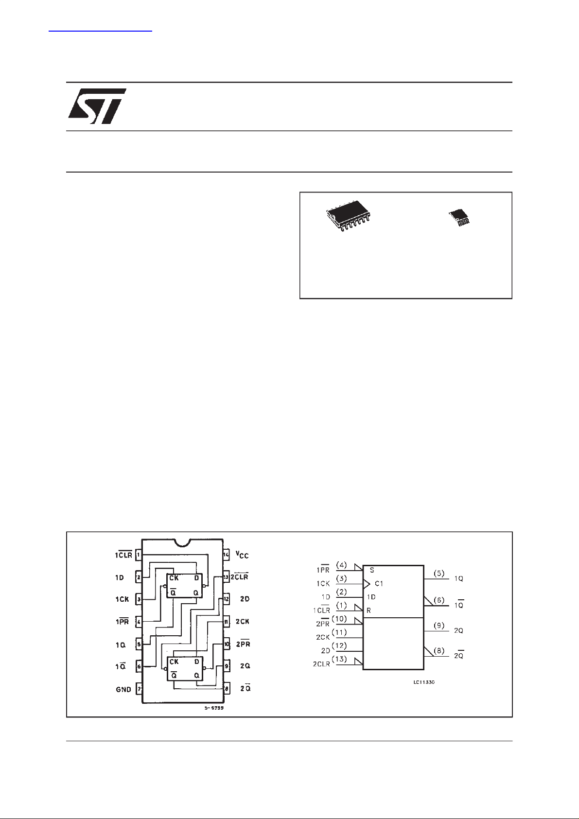
ORDERCODES :
74LVQ74M 74LVQ74T
T
PIN CONNECTION AND IEC LOGICSYMBOLS
February 1999
1/10
74LVQ74
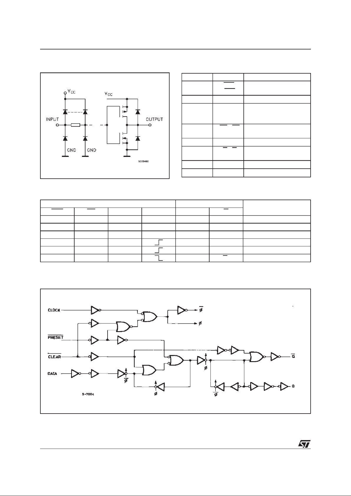
INPUT AND OUTPUT EQUIVALENTCIRCUIT
PIN DESCRIPTION
PI N No SYM BO L NAM E AN D FUNCT I O N
1, 13 1CLR,
2CLR
Asyncronous Reset -
Direct Input
2, 12 1D, 2D Data Inputs
3, 11 1CK, 2CK Clock Input
(LOW-to-HIGH, Edge-
Triggered)
4, 10 1PR, 2PR Asyncronous Set - Direct
Input
5, 9 1Q, 2Q True Flip-Flop Outputs
6, 8 1Q, 2Q Complement Flip-Flop
Outputs
7 GND Ground (0V)
14 V
CC
Positive Supply Voltage
TRUTH TABLE
INP U T S OUT P UTS FUNCTI ON
CLRPRDCKQ Q
L H X X L H CLEAR
H L X X H L PRESET
LLXXHH
HHL LH
HHH HL
HHX Q
X:Don’tCare
n
Q
n
NO CHANGE
LOGICDIAGRAM
Thislogic diagram has notbeused toesimate propagation delays
2/10
74LVQ74
ABSOLUTE MAXIMUM RATINGS
Symb o l Para met er Val u e Un i t
V
V
V
I
I
OK
I
or I
I
CC
T
T
AbsoluteMaximum Ratingsarethosevalues beyondwhichdamage tothedevicemayoccur. Functionaloperationunderthese conditionisnotimplied.
RECOMMENDEDOPERATINGCONDITIONS
Symb o l Para met er Value U n it
V
V
V
T
dt/dv Input Rise and Fall Time (V
1) Truth Table guaranteed: 1.2V to 3.6V
2)V
from0.8Vto2V
IN
Supply Voltage -0.5 to +7 V
CC
DC Input Voltage -0.5 to VCC+ 0.5 V
I
DC Output Voltage -0.5 to VCC+ 0.5 V
O
DC Input Diode Current ± 20 mA
IK
DC Output Diode Current ± 20 mA
DC Output Current
O
DC VCCor Ground Current
GND
Storage Temperature -65 to +150
stg
Lead Temperature (10 sec) 300
L
Supply Voltage (note 1) 2 to 3.6 V
CC
Input Voltage 0 to V
I
Output Voltage 0 to V
O
Operating Temperature: -40 to +85
op
= 3V) (note 2) 0 to 10 ns/V
CC
50 mA
±
400 mA
±
CC
CC
o
C
o
C
V
V
o
C
3/10
74LVQ74
DC SPECIFICATIONS
Symbol Parameter Test Conditions Value Unit
T
V
CC
(V)
High Level Input Voltage
V
IH
Low Level Input Voltage 0.8 0.8 V
V
IL
High Level Output
V
OH
Voltage
Low Level Output
V
OL
Voltage
Input Leakage Current
I
I
Quiescent Supply
I
CC
3.0 to
3.6
3.0 V
3.0 V
3.6
(*)
=
IO=-50 µA 2.9 2.99 2.9
I
or
V
IH
V
IL
(*)
I
V
IH
V
IL
=-12 mA 2.58 2.48
I
O
=-24 mA 2.2
I
O
=
IO=50 µA 0.002 0.1 0.1
or
=12 mA 0 0.36 0.44
I
O
=24 mA 0.55
I
O
VI=VCCor GND ±0.1 ±1 µA
3.6 VI=VCCor GND 2 20
Current
Dynamic Output Current
I
OLD
OHD
(note 1, 2)
I
1) Maximumtest duration 2ms, oneoutput loaded attime
2)Incidentwaveswitchingisguaranteed ontransmissionlineswithimpedances aslowas 50Ω.
(*)Alloutputs loaded.
3.6 V
= 0.8 V max 36 mA
OLD
V
= 2 V min -25 mA
OHD
=25oC -40 t o 85oC
A
Min. Typ. Max. Min. Max.
2.0 2.0
µ
V
V
V
A
DYNAMICSWITCHING CHARACTERISTICS
Symbol Parameter Test Conditions Value Unit
T
V
CC
(V)
V
V
V
Dynamic Low Voltage
OLP
Quiet Output (note 1, 2)
OLV
Dynamic High Voltage
IHD
3.3
3.3 2
C
L
=50pF
Input (note 1, 3)
V
Dynamic Low Voltage
ILD
3.3 0.8
Input (note 1, 3)
1)Worst casepackage
2)Maxnumberofoutputsdefined as(n).Datainputs aredriven0Vto3.3V,(n -1)outputs switching andoneoutputat GND
3)maxnumberofdatainputs(n)switching.(n-1)switching0Vto3.3V.Inputs under testswitching: 3.3Vtothreshold(V
=25oC -40 t o 85oC
A
Min. Typ. Max. Min. Max.
0.2 0.8
-0.8 -0.2
),0Vtothreshold (V
ILD
).f=1MHz
IHD
V
4/10
 Loading...