

查询74LVQ280供应商
74LVQ280
9 BIT PARITY GENERATOR
■ HIGH SPEED:
= 8 ns (TYP.) at VCC = 3.3 V
t
PD
■ COMPA TIBLE WITH TTL OUTPUTS
■ LOW POWER DISSIPATION:
I
= 2µA(MAX.) at TA=25°C
CC
■ LOW NOISE:
= 0.3V (TYP.) at VCC = 3.3V
V
OLP
■ 75Ω TRANSMISSION LINE DRIVING
CAPABILITY
■ SYMMETRICAL OUTPUT IMPEDANCE:
| = IOL = 12mA (MIN) at VCC = 3.0 V
|I
OH
■ PCI BUS LEVELS GUARANTEED AT 24 mA
■ BALANCED PROPAGATION DELAYS:
≅ t
t
PLH
■ OPERATING VOLTAGE RANGE:
V
CC
■ PIN AND FUNCTION COMPATIBLE WITH
PHL
(OPR) = 2V to 3.6V
74 SERIES 280
■ IMPROVED LATCH-U P IMMUNITY
DESCRIPTION
The 74LVQ280 is a low voltage CMOS 9 BIT
PARITY GENERATOR fabricated with sub-micron
silicon gate and double-layer metal wiring C2MOS
technology. It is ideal for low power and low noise
3.3V applications.
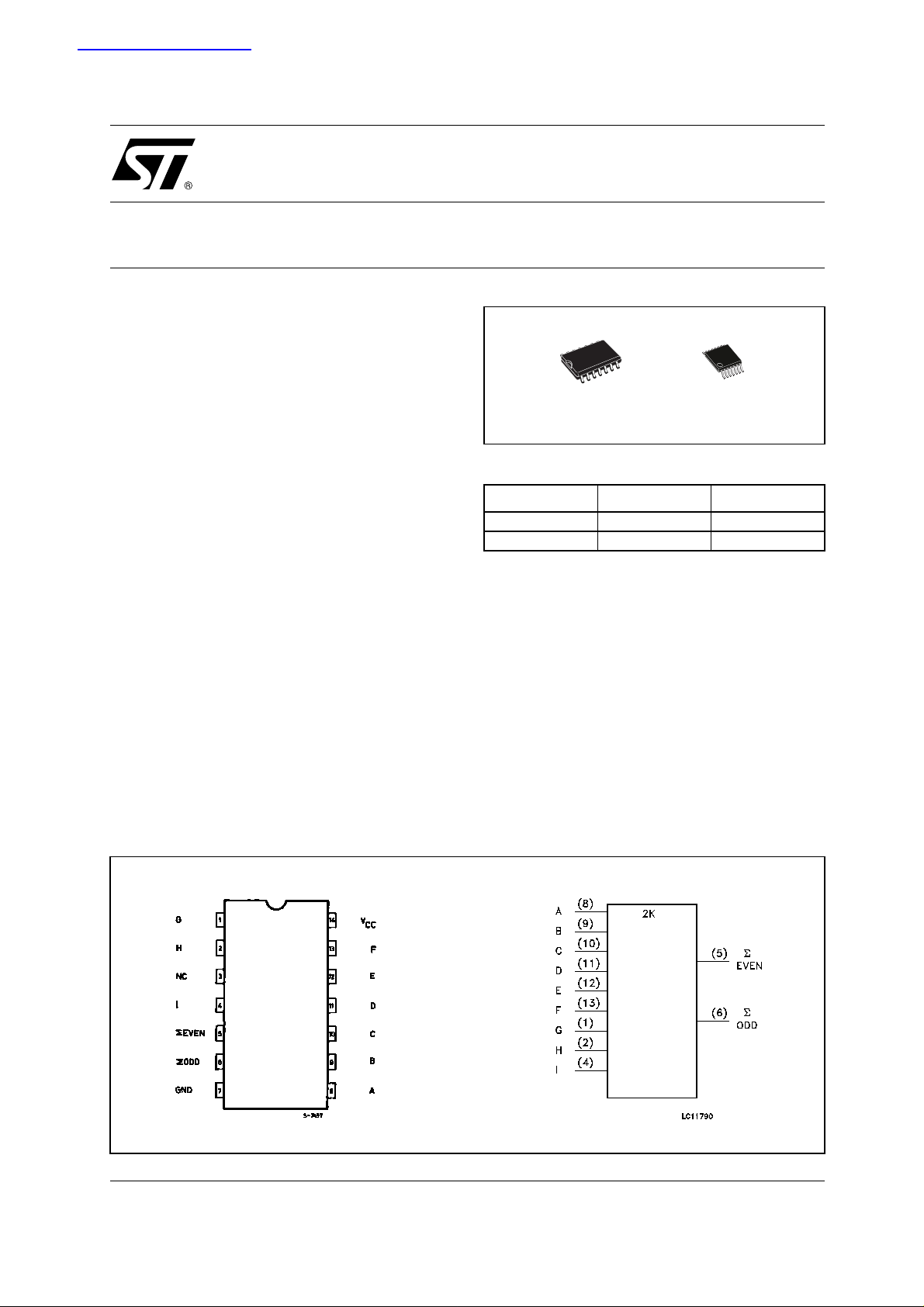
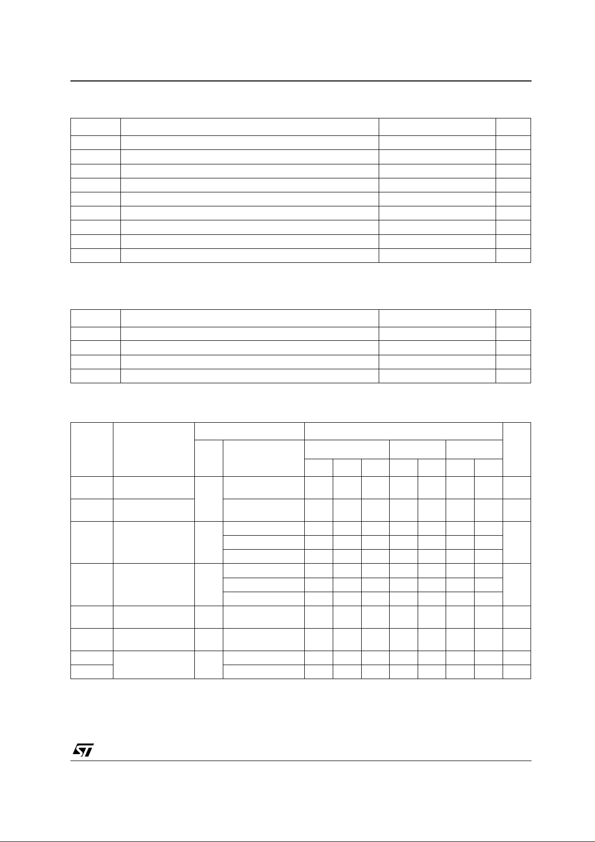
It is composed of nine data inputs (A to I) and odd/
even parity outputs (ΣODD and ΣEVEN). The nine
TSSOPSOP
ORDER CODES
PACKAGE TUBE T & R
SOP 74LVQ280M 74LVQ280MTR
TSSOP 74LVQ280TTR
data inputs control the output conditions. When
the number of high level input is odd, ΣODD
output is kept high and ΣEVEN output low.
Conversely, when the number of high level is
even, ΣEVEN output is kept high and ΣODD low.
The IC generates either odd or even parity making
it flexible application. The word-length capability is
easily expanded by cascading.
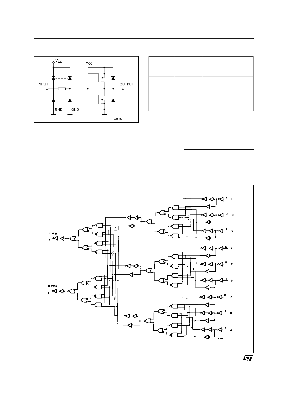
All inputs and outputs are equipped with
protection circuits against stat ic discharge, giving
them 2KV ESD immunity and transient excess
voltage.
PIN CONNECTION AND IEC LOGIC SYMBOLS
1/8July 2001
74LVQ280
INPUT AND OUTPUT EQUIVALENT CIRCUIT PIN DESCRIPTION
PIN No SYMBOL NAME AND FUNCTION
5 ΣEVEN Even Parity Output
6 ΣODD Odd Parity Output
8, 9, 10, 11,
12, 13, 1, 2,
4
3 NC No Connection
7 GND Ground (0V)
14
TRUTH TABLE
A to I Data Inputs
V
CC
Positive Supply Voltage
NUMBER OF INPUTS A - I THAT ARE HIGH
LOGIC DIAGRAM
OUTPUTS
ΣEVEN ΣODD
0, 2, 4, 6, 8 H L
1, 3, 5, 7, 9 L H
2/8
74LVQ280
ABSOLUTE MAXIMUM RATINGS
Symbol Parameter Value Unit
V
V
V
I
I
OK
I
I
or I
CC
T
T
Absolute Maximum Ratings are those values beyond which damage to the device may occur. Functional operation under these conditions is
not implied
RECOMMENDED OPERATING CONDITIONS
Symbol Parameter Value Unit
V
V
V
T
1) Truth T abl e guarante ed: 1.2V to 3.6 V
Supply Voltage
CC
DC Input Voltage -0.5 to VCC + 0.5
I
DC Output Voltage -0.5 to VCC + 0.5
O
DC Input Diode Current
IK
DC Output Diode Current
DC Output Current
O
DC VCC or Ground Current
GND
Storage Temperature
stg
Lead Temperature (10 sec)
L
Supply Voltage (note 1)
CC
Input Voltage 0 to V
I
Output Voltage 0 to V
O
Operating Temperature
op
-0.5 to +7 V
± 20 mA
± 20 mA
± 50 mA
± 300 mA
-65 to +150 °C
300 °C
2 to 3.6 V
CC
CC
-55 to 125 °C
V
V
V
V
DC SPECIFICATIONS
Test Condition Value
T
Symbol Parameter
V
CC
(V)
V
V
V
V
I
I
OLD
I
OHD
1) Maxim um test duration 2ms, one out put loaded at time
2) Incid ent wave sw i tc hi ng is guara nt eed on transmi ssion lines with impedances a s low as 75Ω
High Level Input
IH
Voltage
Low Level Input
IL
Voltage
High Level Output
OH
Voltage
Low Level Output
OL
Voltage
I
Input Leakage
I
Current
Quiescent Supply
CC
Current
Dynamic Output
Current (note 1, 2)
3.0 to
3.6
3.0
3.0
3.6
3.6
3.6
=-50 µA
I
O
I
=-12 mA
O
I
=-24 mA
O
IO=50 µA
I
=12 mA
O
I
=24 mA
O
V
= VCC or GND
I
= VCC or GND
V
I
= 0.8 V max
V
OLD
V
= 2 V min
OHD
= 25°C
A
Min. Typ. Max. Min. Max. Min. Max.
2.0 2.0 2.0 V
0.8 0.8 0.8 V
2.9 2.99 2.9 2.9
2.58 2.48 2.48
0.002 0.1 0.1 0.1
0 0.36 0.44 0.44
± 0.1 ± 1 ± 1 µA
22020µA
-40 to 85°C -55 to 125°C
Unit
2.2 2.2
0.55 0.55
36 25 mA
-25 -25 mA
V
V
3/8
 Loading...