

ST 74LVC573A User Manual

74LVC573A
OCTAL D-TYPE LATCH HIGH PERFORMANCE
■5V TOLERANT INPUTS
■HIGH SPEED: tPD = 6.8ns (MAX.) at VCC = 3V
■POWER DOWN PROTECTION ON INPUTS AND OUTPUTS
■SYMMETRICAL OUTPUT IMPEDANCE: |IOH| = IOL = 24mA (MIN) at VCC = 3V
■PCI BUS LEVELS GUARANTEED AT 24 mA
■BALANCED PROPAGATION DELAYS: tPLH tPHL
■OPERATING VOLTAGE RANGE:
VCC(OPR) = 1.65V to 3.6V (1.2V Data Retention)
■PIN AND FUNCTION COMPATIBLE WITH 74 SERIES 573
■LATCH-UP PERFORMANCE EXCEEDS 500mA (JESD 17)
■ESD PERFORMANCE:
HBM > 2000V (MIL STD 883 method 3015); MM > 200V
DESCRIPTION
The 74LVC573A is a low voltage CMOS OCTAL D-TYPE LATCH fabricated with sub-micron silicon gate and double-layer metal wiring C2MOS technology. It is ideal for 1.65 to 3.6 VCC operations and low power and low noise applications.
These 8 bit D-Type latch are controlled by a latch enable input (LE) and an output enable input (OE). While the LE inputs is held at a high level, the Q
Figure 1: Pin Connection And IEC Logic Symbols
SOP TSSOP
Table 1: Order Codes
PACKAGE |
T & R |
|
|
SOP |
74LVC573AMTR |
|
|
TSSOP |
74LVC573ATTR |
|
|
outputs will follow the data input precisely or inversely. When the LE is taken low, the Q outputs will be latched precisely or inversely at the logic level of D input data. While the (OE) input is low, the 8 outputs will be in a normal logic state (high or low logic level) and while high level the outputs will be in a high impedance state.
This device is designed to interface directly High Speed CMOS systems with TTL and NMOS components. It has more speed performance at 3.3V than 5V AC/ACT family, combined with a lower power consumption.
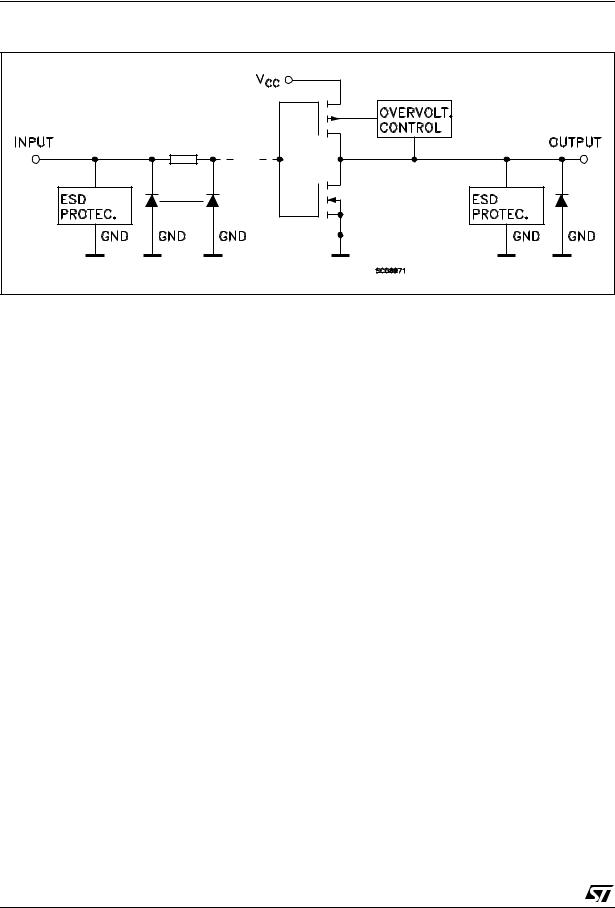
All inputs are equipped with protection circuits against static discharge, giving them 2KV ESD immunity and transient excess voltage.
July 2004 |
Rev. 3 |
1/13 |
|
|
|
74LVC573A
Figure 2: Input And Output Equivalent Circuit
Table 2: Pin Description
PIN N° |
SYMBOL |
NAME AND FUNCTION |
|
|
|
1 |
OE |
3 State Output Enable |
|
|
Input (Active LOW) |
2, 3, 4, 5, 6, |
D0 to D7 |
Data Inputs |
7, 8, 9 |
|
|
|
|
|
12, 13, 14, |
Q0 to Q7 |
3-State Latch Outputs |
15, 16, 17, |
|
|
18, 19 |
|
|
|
|
|
11 |
LE |
Latch Enable Input |
|
|
|
10 |
GND |
Ground (0V) |
|
|
|
20 |
VCC |
Positive Supply Voltage |
Table 3: Truth Table
|
|
|
INPUTS |
|
OUTPUT |
|
|
|
|
|
|
|
OE |
|
LE |
D |
Q |
|
|
|
|
|
|
|
H |
|
X |
X |
Z |
|
|
|
|
|
|
|
L |
|
L |
X |
NO |
|
|
CHANGE |
|||
|
|
|
|
|
|
|
L |
|
H |
L |
L |
|
|
|
|
|
|
|
L |
|
H |
H |
H |
|
|
|
|
|
|
X : Don’t Care
Z : High Impedance
Table 4: Absolute Maximum Ratings
Symbol |
Parameter |
Value |
Unit |
|
|
|
|
|
|
VCC |
Supply Voltage |
-0.5 to +7.0 |
V |
|
VI |
DC Input Voltage |
-0.5 to +7.0 |
V |
|
VO |
DC Output Voltage (VCC = 0V) |
-0.5 to +7.0 |
V |
|
VO |
DC Output Voltage (High or Low State) (note 1) |
-0.5 to VCC + 0.5 |
V |
|
IIK |
DC Input Diode Current |
- 50 |
mA |
|
IOK |
DC Output Diode Current (note 2) |
- 50 |
mA |
|
IO |
DC Output Current |
± |
50 |
mA |
ICC or IGND |
DC VCC or Ground Current per Supply Pin |
± |
100 |
mA |
Tstg |
Storage Temperature |
-65 to +150 |
°C |
|
TL |
Lead Temperature (10 sec) |
300 |
°C |
|
Absolute Maximum Ratings are those values beyond which damage to the device may occur. Functional operation under these conditions is not implied
1)IO absolute maximum rating must be observed
2)VO < GND
2/13

|
|
|
|
74LVC573A |
|
Table 5: Recommended Operating Conditions |
|
|
|
|
|
|
|
|
|
|
|
Symbol |
Parameter |
Value |
|
Unit |
|
|
|
|
|
|
|
VCC |
Supply Voltage (note 1) |
1.65 to 3.6 |
|
V |
|
VI |
Input Voltage |
0 to 5.5 |
|
V |
|
VO |
Output Voltage (VCC = 0V) |
0 to 5.5 |
|
V |
|
VO |
Output Voltage (High or Low State) |
0 to VCC |
|
V |
|
IOH, IOL |
High or Low Level Output Current (VCC = 3.0 to 3.6V) |
± |
24 |
|
mA |
IOH, IOL |
High or Low Level Output Current (VCC = 2.7 to 3.0V) |
± |
12 |
|
mA |
IOH, IOL |
High or Low Level Output Current (VCC = 2.3 to 2.7V) |
± |
8 |
|
mA |
IOH, IOL |
High or Low Level Output Current (VCC = 1.65 to 2.3V) |
± |
4 |
|
mA |
Top |
Operating Temperature |
-55 to 125 |
|
°C |
|
dt/dv |
Input Rise and Fall Time (note 2) |
0 to 10 |
|
ns/V |
|
|
|
|
|
|
|
1)Truth Table guaranteed: 1.2V to 3.6V
2)VIN from 0.8V to 2V at VCC = 3.0V
Table 6: DC Specifications
|
|
Test Condition |
|
Value |
|
|
||
Symbol |
Parameter |
|
|
|
|
|
|
Unit |
VCC |
|
-40 to 85 °C |
-55 to 125 °C |
|||||
|
|
|
|
|
|
|
|
|
|
|
(V) |
|
Min. |
Max. |
Min. |
Max. |
|
|
|
|
|
|
||||
|
|
|
|
|
|
|
|
|
VIH |
High Level Input |
1.65 to 1.95 |
|
0.65VCC |
|
0.65VCC |
|
|
|
Voltage |
|
|
|
|
|
|
V |
|
2.3 to 2.7 |
|
1.7 |
|
1.7 |
|
||
|
|
|
|
|
||||
|
|
2.7 to 3.6 |
|
2 |
|
2 |
|
|
|
|
|
|
|
|
|
|
|
VIL |
Low Level Input |
1.65 to 1.95 |
|
|
0.35VCC |
|
0.35VCC |
|
|
Voltage |
|
|
|
|
|
|
V |
|
2.3 to 2.7 |
|
|
0.7 |
|
0.7 |
||
|
|
|
|
|
||||
|
|
|
|
|
|
|
|
|
|
|
2.7 to 3.6 |
|
|
0.8 |
|
0.8 |
|
|
|
|
|
|
|
|
|
|
VOH |
High Level Output |
1.65 to 3.6 |
IO=-100 A |
VCC-0.2 |
|
VCC-0.2 |
|
|
|
Voltage |
|
|
|
|
|
|
|
|
1.65 |
IO=-4 mA |
1.2 |
|
1.2 |
|
|
|
|
|
|
|
|
||||
|
|
2.3 |
IO=-8 mA |
1.7 |
|
1.7 |
|
V |
|
|
2.7 |
IO=-12 mA |
2.2 |
|
2.2 |
|
|
|
|
|
|
|
||||
|
|
3.0 |
IO=-18 mA |
2.4 |
|
2.4 |
|
|
|
|
3.0 |
IO=-24 mA |
2.2 |
|
2.2 |
|
|
VOL |
Low Level Output |
1.65 to 3.6 |
IO=100 A |
|
0.2 |
|
0.2 |
|
|
Voltage |
|
|
|
|
|
|
|
|
1.65 |
IO=4 mA |
|
0.45 |
|
0.45 |
|
|
|
|
|
|
|
||||
|
|
2.3 |
IO=8 mA |
|
0.7 |
|
0.7 |
V |
|
|
2.7 |
IO=12 mA |
|
0.4 |
|
0.4 |
|
|
|
3.0 |
IO=24 mA |
|
0.55 |
|
0.55 |
|
II |
Input Leakage Current |
3.6 |
VI = 0 to 5.5V |
|
± 5 |
|
± 5 |
A |
Ioff |
Power Off Leakage |
0 |
VI or VO = 5.5V |
|
10 |
|
10 |
A |
|
Current |
|
|
|||||
|
|
|
|
|
|
|
|
|
IOZ |
High Impedance |
3.6 |
VI = VIH or VIL |
|
± 5 |
|
± 5 |
A |
|
Output Leakage |
|
VO = 0 to 5.5V |
|
|
|
|
|
|
Current |
|
|
|
|
|
|
|
ICC |
Quiescent Supply |
|
VI = VCC or GND |
|
10 |
|
10 |
|
|
Current |
3.6 |
|
|
|
|
|
A |
|
VI or VO = 3.6 to |
|
± 10 |
|
± 10 |
|||
|
|
|
|
|||||
|
|
|
5.5V |
|
|
|
||
|
|
|
|
|
|
|
|
|
|
|
|
|
|
|
|
|
|
∆ ICC |
ICC incr. per Input |
2.7 to 3.6 |
VIH = VCC-0.6V |
|
500 |
|
500 |
A |
3/13

74LVC573A
Table 7: Dynamic Switching Characteristics
|
|
|
Test Condition |
|
|
Value |
|
|
|||
|
|
|
|
|
|
|
|
|
|
|
|
Symbol |
Parameter |
VCC |
|
|
|
TA = 25 |
°C |
|
Unit |
||
|
|
(V) |
|
|
Min. |
|
Typ. |
|
|
Max. |
|
|
|
|
|
|
|
|
|
|
|||
|
|
|
|
|
|
|
|
|
|
|
|
VOLP |
Dynamic Low Level Quiet |
3.3 |
|
CL = 50pF |
|
|
0.8 |
|
|
|
V |
|
Output (note 1) |
|
VIL = 0V, VIH = 3.3V |
|
|
|
|
|
|
||
VOLV |
|
|
|
-0.8 |
|
|
|
||||
|
|
|
|
|
|
|
|
|
|||
1) Number of output defined as "n". Measured with "n-1" outputs switching from HIGH to LOW or LOW to HIGH. The remaining output is measured in the LOW state.
Table 8: AC Electrical Characteristics
|
|
|
Test Condition |
|
|
Value |
|
|
|||
Symbol |
Parameter |
|
|
|
|
|
|
|
|
|
Unit |
VCC |
CL |
RL |
ts = tr |
-40 to 85 °C |
-55 to 125 °C |
||||||
|
|
|
|
|
|
|
|||||
|
|
(V) |
|
(pF) |
(Ω ) |
(ns) |
Min. |
Max. |
Min. |
Max. |
|
|
|
|
|
|
|
|
|
||||
|
|
|
|
|
|
|
|
|
|
|
|
tPLH tPHL |
Propagation Delay |
1.65 to |
1.95 |
30 |
1000 |
2.0 |
|
TBD |
|
TBD |
|
|
Time D to Q |
2.3 to |
2.7 |
30 |
500 |
2.0 |
|
TBD |
|
TBD |
ns |
|
|
|
|
|
|
|
|
|
|
|
|
|
|
2.7 |
|
50 |
500 |
2.5 |
1.5 |
7.8 |
1.5 |
9.4 |
|
|
|
|
|
||||||||
|
|
|
|
|
|
|
|
|
|
|
|
|
|
3.0 to |
3.6 |
50 |
500 |
2.5 |
1 |
6.8 |
1 |
8.2 |
|
|
|
|
|
|
|
|
|
|
|
|
|
tPLH tPHL |
Propagation Delay |
1.65 to |
1.95 |
30 |
1000 |
2.0 |
|
TBD |
|
TBD |
|
|
Time LE to Q |
2.3 to |
2.7 |
30 |
500 |
2.0 |
|
TBD |
|
TBD |
ns |
|
|
|
|
|
|
|
|
|
|
|
|
|
|
2.7 |
|
50 |
500 |
2.5 |
1.5 |
7.8 |
1.5 |
9.4 |
|
|
|
|
|
||||||||
|
|
|
|
|
|
|
|
|
|
|
|
|
|
3.0 to |
3.6 |
50 |
500 |
2.5 |
1 |
6.8 |
1 |
8.2 |
|
|
|
|
|
|
|
|
|
|
|
|
|
tPZL tPZH |
Output Enable Time |
1.65 to |
1.95 |
30 |
1000 |
2.0 |
|
TBD |
|
TBD |
|
|
|
2.3 to |
2.7 |
30 |
500 |
2.0 |
|
TBD |
|
TBD |
ns |
|
|
|
|
|
|
|
|
|
|
|
|
|
|
2.7 |
|
50 |
500 |
2.5 |
1 |
8.7 |
1 |
10.4 |
|
|
|
|
|
||||||||
|
|
|
|
|
|
|
|
|
|
|
|
|
|
3.0 to |
3.6 |
50 |
500 |
2.5 |
1 |
7.7 |
1 |
9.2 |
|
|
|
|
|
|
|
|
|
|
|
|
|
tPLZ tPHZ |
Output Disable Time |
1.65 to |
1.95 |
30 |
1000 |
2.0 |
|
TBD |
|
TBD |
|
|
|
2.3 to |
2.7 |
30 |
500 |
2.0 |
|
TBD |
|
TBD |
ns |
|
|
|
|
|
|
|
|
|
|
|
|
|
|
2.7 |
|
50 |
500 |
2.5 |
2 |
7.6 |
2 |
9.1 |
|
|
|
|
|
||||||||
|
|
|
|
|
|
|
|
|
|
|
|
|
|
3.0 to |
3.6 |
50 |
500 |
2.5 |
2 |
7.0 |
2 |
8.4 |
|
|
|
|
|
|
|
|
|
|
|
|
|
tW |
LE Pulse Width |
1.65 to |
1.95 |
30 |
1000 |
2.0 |
TBD |
|
TBD |
|
|
|
HIGH |
2.3 to |
2.7 |
30 |
500 |
2.0 |
TBD |
|
TBD |
|
ns |
|
|
|
|
|
|
|
|
|
|
|
|
|
|
2.7 |
|
50 |
500 |
2.5 |
3.3 |
|
3.3 |
|
|
|
|
|
|
|
|
||||||
|
|
|
|
|
|
|
|
|
|
|
|
|
|
3.0 to |
3.6 |
50 |
500 |
2.5 |
3.3 |
|
3.3 |
|
|
|
|
|
|
|
|
|
|
|
|
|
|
ts |
Setup Time D to LE, |
1.65 to |
1.95 |
30 |
1000 |
2.0 |
TBD |
|
TDB |
|
|
|
(HIGH to LOW) |
2.3 to |
2.7 |
30 |
500 |
2.0 |
TBD |
|
TBD |
|
ns |
|
|
|
|
||||||||
|
|
|
|
|
|
|
|
|
|
|
|
|
|
2.7 |
|
50 |
500 |
2.5 |
2 |
|
2 |
|
|
|
|
|
|
|
|
||||||
|
|
|
|
|
|
|
|
|
|
|
|
|
|
3.0 to |
3.6 |
50 |
500 |
2.5 |
2 |
|
2 |
|
|
|
|
|
|
|
|
|
|
|
|
|
|
th |
Hold Time LE (HIGH |
1.65 to |
1.95 |
30 |
1000 |
2.0 |
TBD |
|
TBD |
|
|
|
to LOW) to D |
2.3 to |
2.7 |
30 |
500 |
2.0 |
TBD |
|
TBD |
|
ns |
|
|
|
|
|
|
|
|
|
|
|
|
|
|
2.7 |
|
50 |
500 |
2.5 |
1.5 |
|
1.5 |
|
|
|
|
|
|
|
|
||||||
|
|
|
|
|
|
|
|
|
|
|
|
|
|
3.0 to |
3.6 |
50 |
500 |
2.5 |
1.5 |
|
1.5 |
|
|
|
|
|
|
|
|
|
|
|
|
|
|
tOSLH |
Output To Output |
2.7 to |
3.6 |
|
|
|
|
1 |
|
1 |
ns |
tOSHL |
Skew Time (note1, |
|
|
|
|
|
|
|
|
|
|
|
2) |
|
|
|
|
|
|
|
|
|
|
1) Skew is defined as the absolute value of the difference between the actual propagation delay for any two outputs of the same device switch-
ing in the same direction, either HIGH or LOW (tOSLH = | tPLHm - tPLHn|, tOSHL = | tPHLm - tPHLn| 2) Parameter guaranteed by design
4/13
 Loading...