

74LVC374A
OCTAL D-TYPE FLIP-FLOP
HIGH PERFORMANCE
■ 5V TOLERANT INPUTS
■ HIGH SPEED: t
■ POWER DOWN PROTECTION ON INPUTS
= 6.8ns (MAX.) at VCC = 3V
PD
AND OUTPUTS
■ SYMMETRICAL OUTPUT IMPEDANCE:
|I
| = IOL = 24mA (MIN) at VCC = 3V
OH
■ PCI BUS LEVELS GUARANTEED AT 24 mA
■ BALANCED PROPAGATION DELAYS:
t
≅ t
PLH
■ OPERATING VOLTAGE RANGE:
V
CC
PHL
(OPR) = 1.65V to 3.6V (1.2V Data
Retention)
■ PIN AND FUNCTION COMPATIBLE WITH
74 SERIES 374
■ LA TCH-UP PERFORMANCE EXCEEDS
500mA (JESD 17)
■ ESD PERFORMANCE:
HBM > 2000V (MIL STD 883 method 3015);
MM > 200V
DESCRIPTION
The 74LVC374A is an advanced high-speed
CMOS OCT AL D- TYP E FL I P FL O P wi th 3 S TAT E
OUTPUTS NON INVERTING fabricated with
sub-micron silicon gate and double-layer metal
wiring C
2
MOS technology.
These 8 bit D-Type latch are controlled by a clock
input (CK) and an output enable input (OE
).
On the positive transition of the clock, the Q
outputs will be set to the logic state that were
setup at the D inputs.
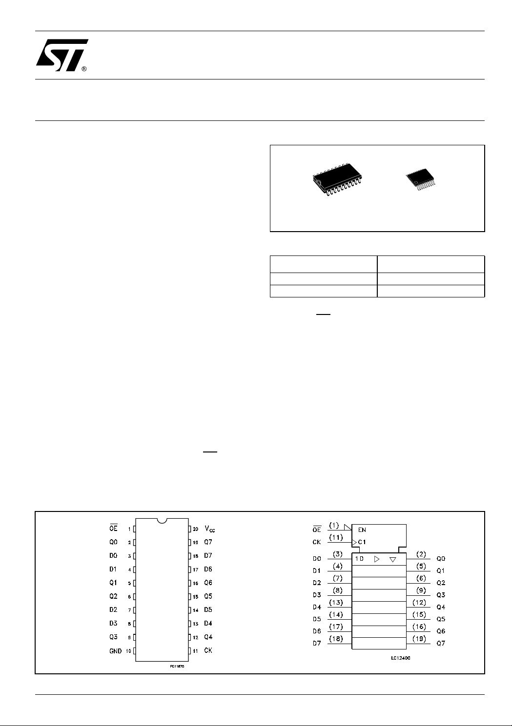
Figure 1: Pin C onnection And I EC Logic Symbol s
TSSOPSOP
Table 1: Order Codes
PACKAGE T & R
SOP 74LVC374AMTR
TSSOP 74LVC374ATTR
While the (OE
) input is low, the 8 outputs will be in
a normal logic state (high or low logic level) and
while high level the outputs will be in a high
impedance state.
The Output control does not affect the internal
operation of flip flops; that is, the old data can be
retained or the new data can be entered even
while the outputs are off. Power down protection is
provided on all inputs and 0 to 7V can be accepted
on inputs with no regard to the supply voltage.
This device can be used to interface 5V to 3V.
All inputs and outputs are equipped with
protection circuits against static disc harge, giving
them 2KV ESD immunity and transient excess
voltage.
Rev. 2
1/14July 2004
74LVC374A
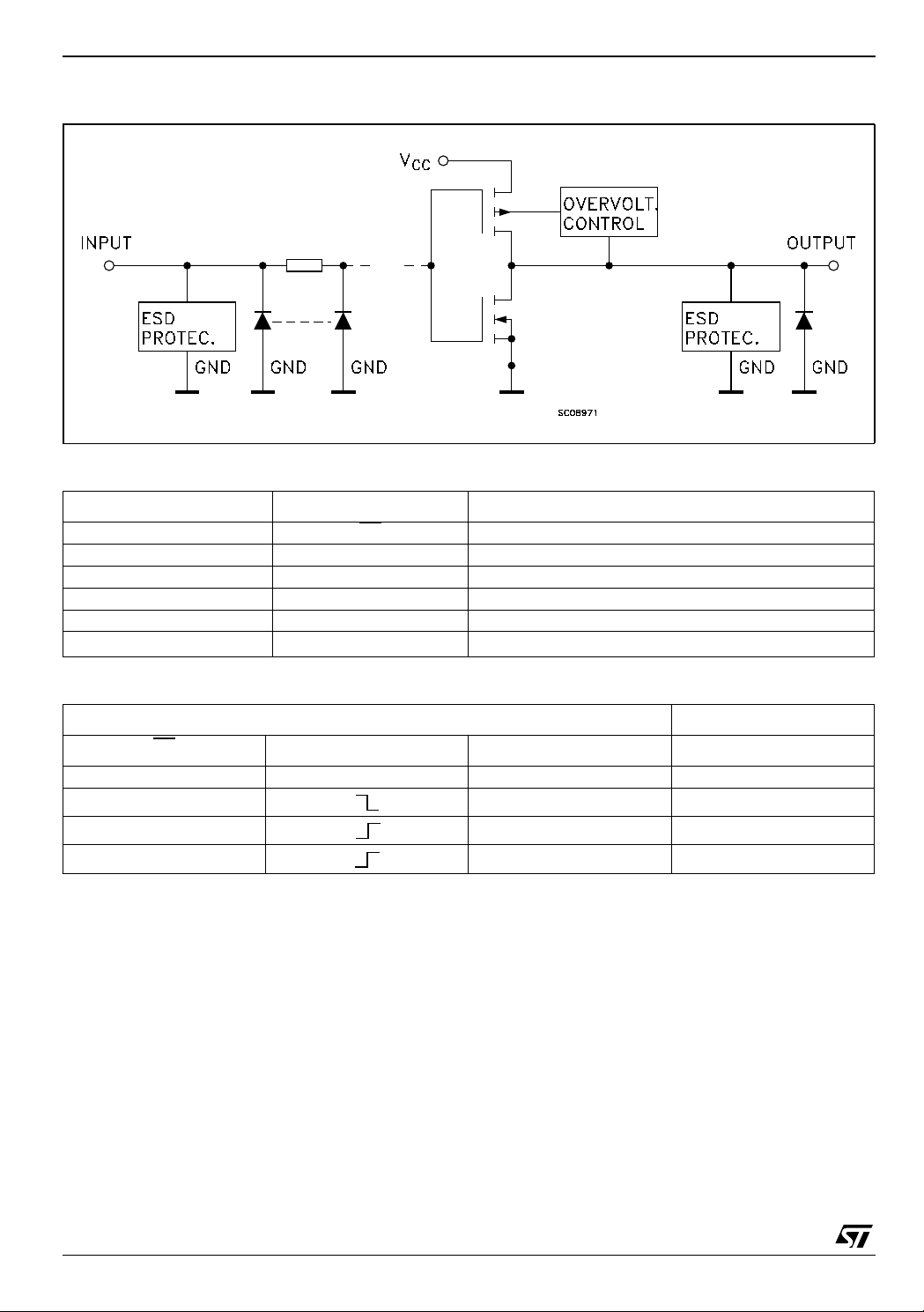
Figure 2: Input An d Output Equival e n t Ci rcui t
Table 2: Pin Description
PIN N° SYMBOL NAME AND FUNCTION
1OE3 State Output Enable Input (Active LOW)
2, 5, 6, 9, 12, 15, 16,19 Q0 to Q7 3-State Outputs
3, 4, 7, 8, 13, 14, 17, 18 D0 to D7 Data Inputs
11 CK Clock
10 GND Ground (0V)
20 V
CC
Positive Supply Voltage
Table 3: Truth Table
OE
HXXZ
L X NO CHANGE
LLL
LHH
X : Don’t Care
Z :High Imp edance
INPUTS OUTPUT
CK D Q
2/14
74LVC374A
Table 4: Absolute Maximum Ratings
Symbol Parameter Value Unit
V
V
V
V
I
I
OK
I
or I
I
CC
T
T
Absolute Maximum Ratings are those values beyond which damage to the device may occur. Functional operation under these conditions is
not implied
absolute maximum rating must be observed
1) I
O
2) V
< GND
O
Table 5: Recommended Operating Conditions
Symbol Parameter Value Unit
V
V
V
V
I
OH
I
OH
I
OH
I
OH
T
dt/dv Input Rise and Fall Time (note 2) 0 to 10 ns/V
Supply Voltage
CC
DC Input Voltage
I
DC Output Voltage (VCC = 0V)
O
DC Output Voltage (High or Low State) (note 1) -0.5 to VCC + 0.5
O
DC Input Diode Current
IK
DC Output Diode Current (note 2)
DC Output Current
O
DC VCC or Ground Current per Supply Pin
GND
Storage Temperature
stg
Lead Temperature (10 sec)
L
Supply Voltage (note 1)
CC
Input Voltage
I
Output Voltage (VCC = 0V)
O
Output Voltage (High or Low State) 0 to V
O
, I
High or Low Level Output Current (VCC = 3.0 to 3.6V)
OL
, I
High or Low Level Output Current (VCC = 2.7 to 3.0V)
OL
, I
High or Low Level Output Current (VCC = 2.3 to 2.7V)
OL
, I
High or Low Level Output Current (VCC = 1.65 to 2.3V)
OL
Operating Temperature
op
-0.5 to +7.0 V
-0.5 to +7.0 V
-0.5 to +7.0 V
V
- 50 mA
- 50 mA
± 50 mA
± 100 mA
-65 to +150 °C
300 °C
1.65 to 3.6 V
0 to 5.5 V
0 to 5.5 V
CC
V
± 24 mA
± 12 mA
± 8mA
± 4mA
-55 to 125 °C
1) Truth T abl e guarante ed: 1.2V to 3.6V
2) V
from 0.8V to 2V at VCC = 3.0V
I
3/14
74LVC374A
Table 6: DC Specifications
Test Condition Value
Symbol Parameter
V
V
V
V
I
I
OZ
High Level Input
IH
Voltage
Low Level Input
IL
Voltage
High Level Output
OH
Voltage
Low Level Output
OL
Voltage
Input Leakage
I
I
Current
Power Off Leakage
off
Current
High Impedance
Output Leakage
Current
I
CC
∆I
Quiescent Supply
Current
ICC incr. per Input
CC
V
CC
(V)
1.65 to 1.95
-40 to 85 °C -55 to 125 °C
Min. Max. Min. Max.
0.65V
CC
0.65V
CC
2.3 to 2.7 1.7 1.7
2.7 to 3.6 2 2
1.65 to 1.95
0.35V
CC
0.35V
2.3 to 2.7 0.7 0.7
2.7 to 3.6 0.8 0.8
=-100 µAVCC-0.2 VCC-0.2
1.65 to 3.6
1.65
2.3
2.7
3.0
3.0
1.65 to 3.6
1.65
2.3
2.7
3.0
3.6
0
3.6 VI = VIH or VIL
3.6
2.7 to 3.6
I
O
=-4 mA
I
O
I
=-8 mA
O
I
=-12 mA
O
=-18 mA
I
O
=-24 mA
I
O
IO=100 µA
I
=4 mA
O
=8 mA
I
O
=12 mA
I
O
=24 mA
I
O
= 0 to 5.5V
V
I
or VO = 5.5V
V
I
V
= 0 to 5.5V
O
VI = VCC or GND
or VO = 3.6 to
V
I
5.5V
VIH = VCC-0.6V
1.2 1.2
1.7 1.7
2.2 2.2
2.4 2.4
2.2 2.2
0.2 0.2
0.45 0.45
0.7 0.7
0.4 0.4
0.55 0.55
± 5 ± 5 µA
10 10 µA
± 10 ± 10 µA
10 10
± 10 ± 10
500 500 µA
Unit
V
CC
V
V
V
µA
Table 7: Dynamic Switching Characteristics
Test Condition Value
= 25 °C
Symbol Parameter
V
CC
(V)
V
OLP
V
OLV
1) Number of output de fined as "n". M easured with "n -1" outputs switching fr om HI GH to LOW or LOW to HIGH. The rem ai ning output is
measur ed i n the LOW state.
Dynamic Low Level Quiet
Output (note 1)
3.3
= 50pF
C
L
V
= 0V, VIH = 3.3V
IL
4/14
T
A
Min. Typ. Max.
0.8
-0.8
Unit
V
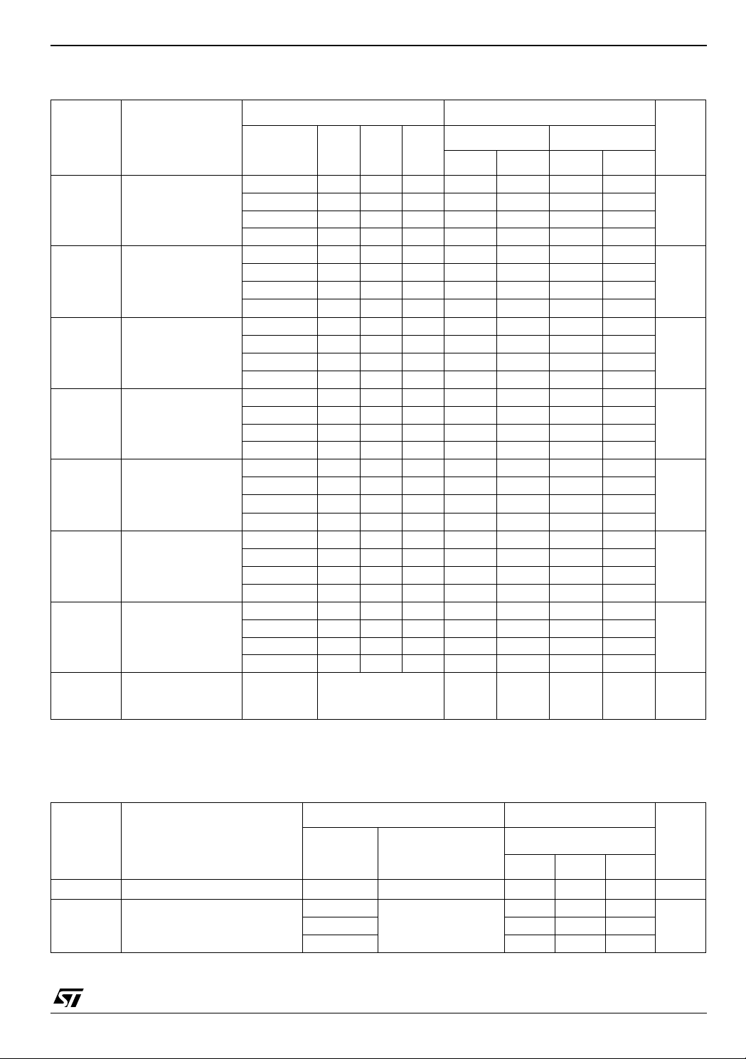
Table 8: AC Electrical Characteristics
Test Condition Value
74LVC374A
Symbol Parameter
t
PLH tPHL
t
PLH tPHL
t
PZL tPZH
t
PLZ tPHZ
t
t
t
Propagation Delay
Time D to Q
Propagation Delay
Time LE to Q
Output Enable Time 1.65 to 1.95 30 1000 2.0 TBD TBD
Output Disable Time 1.65 to 1.95 30 1000 2.0 TBD TBD
LE Pulse Width
W
HIGH
Setup Time D to LE
s
(HIGH to LOW)
Hold Time D to
h
CLOCK, HIGH or
LOW
t
OSLH
t
OSHL
Output To Output
Skew Time (note1,
2)
-40 to 85 °C -55 to 125 °C
V
(V)
CC
C
(pF)
R
L
(Ω)
= t
t
L
s
r
(ns)
Min. Max. Min. Max.
1.65 to 1.95 30 1000 2.0 TBD TBD
2.3 to 2.7 30 500 2.0 TBD TBD
2.7 50 500 2.5 1.5 7.8 1.5 9.4
3.0 to 3.6 50 500 2.5 1 6.8 1 8.2
1.65 to 1.95 30 1000 2.0 TBD TBD
2.3 to 2.7 30 500 2.0 TBD TBD
2.7 50 500 2.5 1.5 7.8 1.5 9.4
3.0 to 3.6 50 500 2.5 1 6.8 1 8.2
2.3 to 2.7 30 500 2.0 TBD TBD
2.7 50 500 2.5 1 8.7 1 10.4
3.0 to 3.6 50 500 2.5 1 7.7 1 9.2
2.3 to 2.7 30 500 2.0 TBD TBD
2.7 50 500 2.5 2 7.6 2 9.1
3.0 to 3.6 50 500 2.5 2 7.0 2 8.4
1.65 to 1.95 30 1000 2.0 TBD TBD
2.3 to 2.7 30 500 2.0 TBD TBD
2.7 50 500 2.5 3.3 3.3
3.0 to 3.6 50 500 2.5 3.3 3.3
1.65 to 1.95 30 1000 2.0 TBD TDB
2.3 to 2.7 30 500 2.0 TBD TBD
2.7 50 500 2.5 2 2
3.0 to 3.6 50 500 2.5 2 2
1.65 to 1.95 30 1000 2.0 TBD TBD
2.3 to 2.7 30 500 2.0 TBD TBD
2.7 50 500 2.5 1.5 1.5
3.0 to 3.6 50 500 2.5 1.5 1.5
2.7 to 3.6 1 1 ns
Unit
ns
ns
ns
ns
ns
ns
ns
1) Skew is defined as the absolute value of the difference between the actual propagation delay for any two outputs of the same device switching in the sa me directio n, either HIGH or LOW (t
2) Param eter guaran teed by design
OSLH
= | t
PLHm
- t
PLHn
|, t
OSHL
= | t
PHLm
- t
PHLn
|
Table 9: Capacitive Characteristics
Test Condition Value
= 25 °C
Symbol Parameter
V
CC
(V)
C
C
Input Capacitance
IN
Power Dissipation Capacitance
PD
(note 1)
1.8 fIN = 10MHz 28
3.3 34
1) CPD is defined as the value of the IC’s internal equivalent capacitance which is calculated from the operating current consumption without
load. (Refer to Test Circuit). Average operating current can be obtained by the following equation. I
CC(opr)
T
A
Min. Typ. Max.
4pF
= CPD x VCC x fIN + ICC/n (per c ircuit )
Unit
pF2.5 30
5/14

74LVC374A
Figure 3: Test Circuit
RT = Z
of pulse generator (typically 50Ω)
OUT
Table 10: Test Circuit And Waveform Symbol Value
Symbol
C
L
R
L = R1
V
S
V
IH
V
M
V
OH
V
X
V
Y
= t
t
r
r
1.65 to 1.95V 2.3 to 2.7V 2.7V 3.0 to 3.6V
30pF 30pF 50pF 50pF
1000Ω 500Ω 500Ω 500Ω
2 x V
V
CC
CC
2 x V
V
CC
CC
VCC/2 VCC/2 1.5V 1.5V
V
CC
V
+ 0.15V V
OL
V
- 0.15V V
OH
V
CC
+ 0.15V V
OL
- 0.15V V
OH
<2.0ns <2.0ns <2.5ns <2.5ns
V
CC
6V 7V
2.7V 3.0V
3.0V 3.5V
+ 0.3V V
OL
- 0.3V V
OH
OL
OH
+ 0.3V
- 0.3V
6/14

74LVC374A
Figure 4: Waveform - Propagation Delay, Setup And Hold Times (f=1MHz; 50% duty cycle)
Figure 5: Waveform - Output Enable And Disable Times (f=1MHz; 50% duty cycle)
7/14

74LVC374A
Figure 6: Waveform - Propagation Delay Time (f=1MHz; 50% duty cycle)
8/14

SO-20 MECHANICAL DATA
74LVC374A
DIM.
A 2.35 2.65 0.093 0.104
A1 0.1 0.30 0.004 0.012
B 0.33 0.51 0.013 0.020
C 0.23 0.32 0.009 0.013
D 12.60 13.00 0.496 0.512
E 7.4 7.6 0.291 0.299
e 1.27 0.050
H 10.00 10.65 0.394 0.419
h 0.25 0.75 0.010 0.030
L 0.4 1.27 0.016 0.050
k0° 8° 0° 8°
ddd 0.100 0.004
MIN. TYP MAX. MIN. TYP. MAX.
mm. inch
0016022D
9/14

74LVC374A
TSSOP20 MECHANICAL DATA
mm. inch
DIM.
MIN. TYP MAX. MIN. TYP. MAX.
A 1.2 0.047
A1 0.05 0.15 0.002 0.004 0.006
A2 0.8 1 1.05 0.031 0.039 0.041
b 0.19 0.30 0.007 0.012
c 0.09 0.20 0.004 0.0079
D 6.4 6.5 6.6 0.252 0.256 0.260
E 6.2 6.4 6.6 0.244 0.252 0.260
E1 4.3 4.4 4.48 0.169 0.173 0.176
e 0.65 BSC 0.0256 BSC
K0˚ 8˚0˚ 8˚
L 0.45 0.60 0.75 0.018 0.024 0.030
A2
A
A1
b
e
K
c
L
E
D
E1
PIN 1 IDENTIFICATION
10/14
1
0087225C

74LVC374A
Tape & Reel SO-20 MECHANICAL
mm. inch
DIM.
MIN. TYP MAX. MIN. TYP. MAX.
A 330 12.992
C 12.8 13.2 0.504 0.519
D 20.2 0.795
N 60 2.362
T 30.4 1.197
Ao 10.8 11 0.425 0.433
Bo 13.2 13.4 0.520 0.528
Ko 3.1 3.3 0.122 0.130
Po 3.9 4.1 0.153 0.161
P 11.9 12.1 0.468 0.476
DATA
11/14

74LVC374A
Tape & Reel TSSOP20 MECHANICAL DATA
mm. inch
DIM.
MIN. TYP MAX. MIN. TYP. MAX.
A 330 12.992
C 12.8 13.2 0.504 0.519
D 20.2 0.795
N 60 2.362
T 22.4 0.882
Ao 6.8 7 0.268 0.276
Bo 6.9 7.1 0.272 0.280
Ko 1.7 1.9 0.067 0.075
Po 3.9 4.1 0.153 0.161
P 11.9 12.1 0.468 0.476
12/14

Table 11: Revision History
Date Revision Description of Change s
21-May-2004 1 First Release.
26-Jul-2004 2 Ordering Codes Revision - pag. 1.
74LVC374A
13/14

74LVC374A
Information furnished is believed to be accurate and reliable. However, STMicroelectronics assumes no responsibility for the consequences
of use of s uch inf ormati on nor for a ny infr ing eme nt o f p atent s or o ther ri ghts of third parti es wh ich m ay res ult fr om i ts us e. No li cens e i s gr an ted
by implication or otherwise under any patent or patent rights of STMicroelectronics. Specifications mentioned in this publication are subject
to change without notice. This publication supersedes and replaces all information previously supplied. STMicroelectronics products are not
authorized for use as critical components in life support devices or systems without express written approval of STMicroelectronics.
The ST logo is a registered trademark of STMicroelectronics
All other names are the property of their respective owners
© 2004 STMicroelectronics - All Rights Reserved
STMicroelectronics group of companies
Australia - Belgium - Brazil - Canada - China - Czech Republic - Finland - France - Germany - Hong Kong - India - Israel - Italy - Japan -
Malaysia - Malta - Morocco - Singapore - Spain - Sweden - Switzerland - United Kingdom - United States of America
www.st.com
14/14
 Loading...