

■ 5V TOLERANTINPUTS
■ HIGH SPEED:t
■ POWER DOWN PROTECTION ON INPUTS
= 6.8ns (MAX.) atVCC=3V
PD
AND OUTPUTS
■ SYMMETRICAL OUTPUT IMPEDANCE:
|IOH|=IOL= 24mA (MIN) at VCC=3V
■ PCI BUS LEVELS GUARANTEED AT24 mA
■ BALANCED PROPAGATION DELAYS:
t
≅ t
PLH
PHL
■ OPERATING VOLTAGE RANGE:
VCC(OPR) = 1.65V to 3.6V (1.2V Data
Retention)
■ PIN AND FUNCTION COMPATIBLE WITH
74 SERIES 373
■ LATCH-UP PERFORMANCE EXCEEDS
500mA (JESD 17)
■ ESD PERFORMANCE:
HBM > 2000V (MIL STD 883 method 3015);
MM > 200V
DESCRIPTION
The 74LVC373A is a low voltage CMOS OCTAL
D-TYPE LATCH fabricated with sub-micron silicon
gate and double-layer metal wiring C2MOS
technology. It is ideal for 1.65 to 3.6 V
CC
operations and low power and low noise
applications.
These 8 bit D-Type latch are controlled by a latch
enable input(LE) and an output enable input (OE).
While the LE inputs is held at a high level, the Q
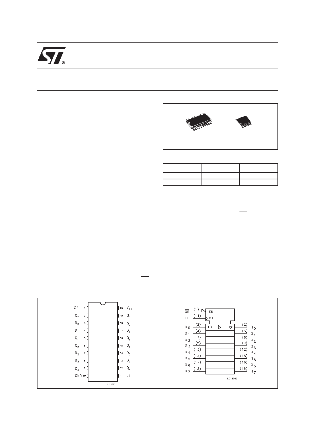
PIN CONNECTION AND IEC LOGIC SYMBOLS
74LVC373A
OCTAL D-TYPE LATCH
HIGH PERFORMANCE
TSSOPSOP
ORDER CODES
PACKAGE TUBE T & R
SOP 74LVC373AM 74LVC373AMTR
TSSOP 74LVC373ATTR
outputs will follow the data input precisely or
inversely. When the LE is taken low,the Q outputs
will be latched precisely or inversely at the logic
level of D input data. While the (OE) input is low,
the 8outputs will be in a normal logic state (high or
low logic level) and while highlevel the outputs will
be in a high impedance state.
This device is designed to interface directly High
Speed CMOS systems with TTL and NMOS
components.
It has more speed performance at 3.3V than 5V
AC/ACT family, combined with a lower power
consumption.
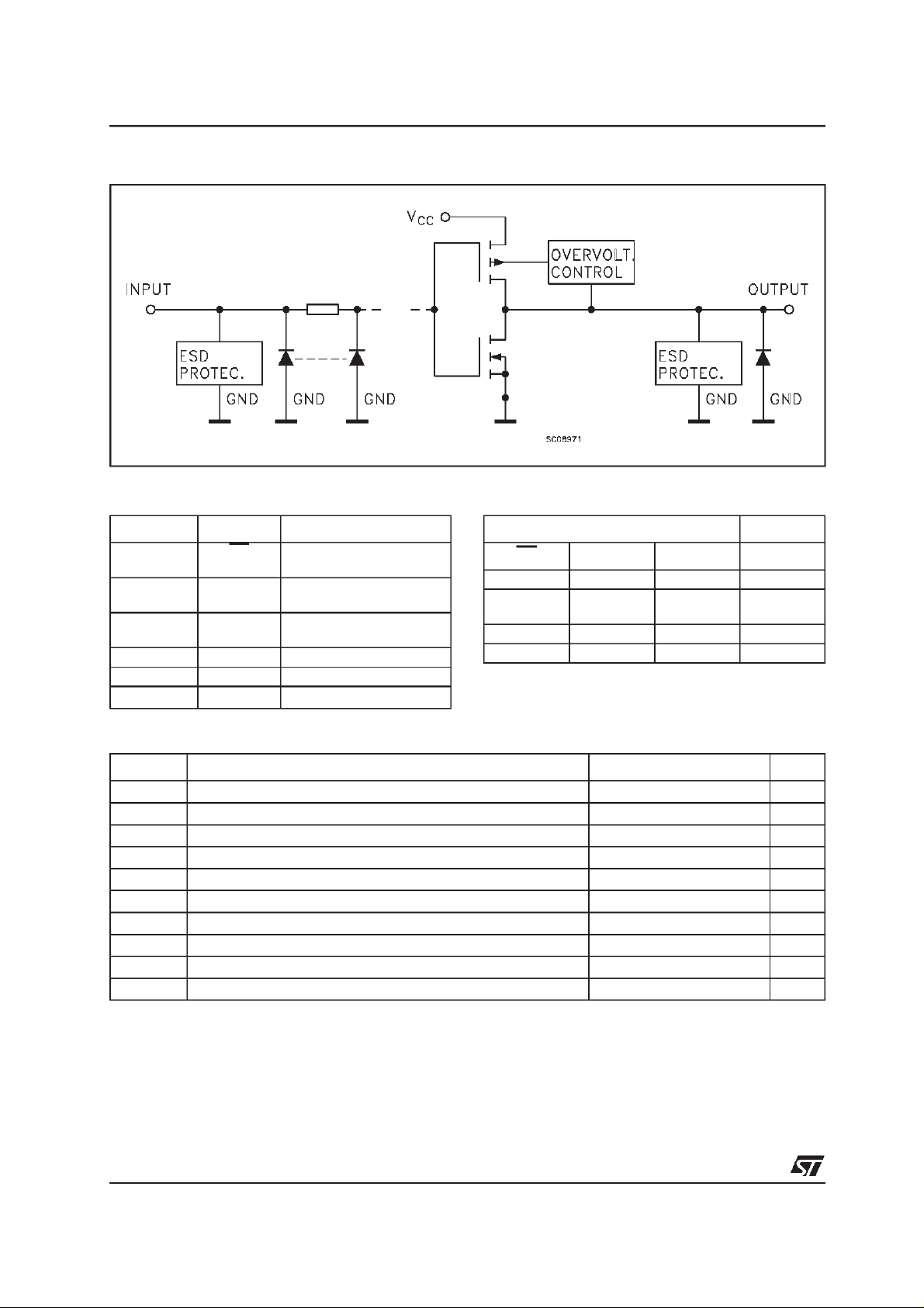
All inputs are equipped with protection circuits
against static discharge, giving them 2KV ESD
immunity and transient excess voltage.
1/10February 2002
74LVC373A
INPUT AND OUTPUT EQUIVALENT CIRCUIT
PIN DESCRIPTION TRUTH TABLE
PIN No SYMBOL NAME AND FUNCTION
1 OE Asynchronous Master
Reset (Active LOW)
2, 5,6, 9, 12,
Q0 to Q7 3-State Outputs
15, 16,19
3, 4,7, 8, 13,
D0 to D7 Data Inputs
14, 17, 18
11 LE Latch Enable Input
10 GND Ground (0V)
20 V
CC
Positive Supply Voltage
OE LE D Q
HXXZ
LLX
LHLL
LHHH
X : Don’t Care
Z :High Impedance
INPUTS OUTPUT
NO
CHANGE
ABSOLUTE MAXIMUM RATINGS
Symbol Parameter Value Unit
V
V
V
V
I
I
OK
I
or I
I
CC
T
T
Absolute Maximum Ratings are those values beyond which damage to thedevice may occur. Functional operation under these conditions is
not implied
absolute maximum rating must be observed
1) I
O
< GND
2) V
O
Supply Voltage
CC
DC Input Voltage
I
DC Output Voltage (VCC= 0V)
O
DC Output Voltage (High or Low State) (note 1) -0.5 to VCC+ 0.5
O
DC Input Diode Current
IK
DC Output Diode Current (note 2)
DC Output Current
O
DC VCCor Ground Current per Supply Pin
GND
Storage Temperature
stg
Lead Temperature (10 sec)
L
-0.5 to +7.0 V
-0.5 to +7.0 V
-0.5 to +7.0 V
V
-50 mA
-50 mA
± 50 mA
± 100 mA
-65 to +150 °C
300 °C
2/10
74LVC373A
RECOMMENDED OPERATING CONDITIONS
Symbol Parameter Value Unit
V
V
V
V
I
OH,IOL
I
OH,IOL
I
OH,IOL
I
OH,IOL
T
dt/dv Input Rise and Fall Time (note 2) 0 to 10 ns/V
1) Truth Table guaranteed: 1.2V to 3.6V
from 0.8V to 2V at VCC= 3.0V
2) V
IN
DC SPECIFICATIONS
Supply Voltage (note 1)
CC
Input Voltage
I
Output Voltage (VCC= 0V)
O
Output Voltage (High or Low State) 0 to V
O
High or Low Level Output Current (VCC= 3.0 to 3.6V)
High or Low Level Output Current (VCC= 2.7 to 3.0V)
High or Low Level Output Current (VCC= 2.3 to 2.7V)
High or Low Level Output Current (VCC= 1.65 to 2.3V)
Operating Temperature
op
Test Condition Value
1.65 to 3.6 V
0 to 5.5 V
0 to 5.5 V
CC
± 24 mA
± 12 mA
± 8mA
± 4mA
-55 to 125 °C
V
Symbol Parameter
V
V
V
V
I
off
I
OZ
High Level Input
IH
Voltage
Low Level Input
IL
Voltage
High Level Output
OH
Voltage
Low Level Output
OL
Voltage
Input Leakage
I
I
Current
Power Off Leakage
Current
High Impedance
Output Leakage
Current
Quiescent Supply
Current
ICCincr. per Input
CC
∆I
I
CC
V
CC
(V)
1.65 to 1.95
-40 to 85 °C -55 to 125 °C
Min. Max. Min. Max.
0.65V
CC
0.65V
CC
2.3 to 2.7 1.7 1.7
2.7 to 3.6 2 2
1.65 to 1.95
0.35V
CC
0.35V
2.3 to 2.7 0.7 0.7
2.7 to 3.6 0.8 0.8
I
1.65 to 3.6
1.65
2.3
2.7
3.0
3.0
1.65 to 3.6
1.65
2.3
2.7
3.0
3.6
0
3.6 VI=VIHorV
=-100 µAVCC-0.2 VCC-0.2
O
I
=-4 mA
O
I
=-8 mA
O
=-12 mA
I
O
=-18 mA
I
O
=-24 mA
I
O
IO=100 µA
I
=4 mA
O
=8 mA
I
O
=12 mA
I
O
=24 mA
I
O
V
= 0 to 5.5V
I
V
or VO= 5.5V
I
IL
1.2 1.2
1.7 1.7
2.2 2.2
2.4 2.4
2.2 2.2
0.2 0.2
0.45 0.45
0.7 0.7
0.4 0.4
0.55 0.55
± 5 ± 5 µA
10 10 µA
± 10 ± 10 µA
VO= 0 to 5.5V
3.6
2.7 to 3.6
VI=VCCor GND
or VO= 3.6 to
V
I
5.5V
VIH=VCC-0.6V
10 10
± 10 ± 10
500 500 µA
Unit
V
CC
V
V
V
µA
3/10
 Loading...