

74LVC245A
LOW VOLTAGE CMOS OCTAL BUS TRANSCEIVER
(NOT INVERTED) HIGH PERFORMANCE
■ 5V TOLERANT INPUTS
■ HIGH SPEED: t
■ POWER DOWN PROTECTION ON INPUTS
= 6.3ns (MAX.) at VCC = 3V
PD
AND OUTPUTS
■ SYMMETRICAL OUTPUT IMPEDANCE:
|I
| = IOL = 24mA (MIN) at VCC = 3V
OH
■ PCI BUS LEVELS GUARANTEED AT 24 mA
■ BALANCED PROPAGATION DELAYS:
t
≅ t
PLH
■ OPERATING VOLTAGE RANGE:
V
CC
PHL
(OPR) = 1.65V to 3.6V (1.2V Data
Retention)
■ PIN AND FUNCTION COMPATIBLE WITH
74 SERIES 245
■ LA TCH-UP PERFORMANCE EXCEEDS
500mA (JESD 17)
■ ESD PERFORMANCE:
HBM > 2000V (MIL STD 883 method 3015);
MM > 200V
DESCRIPTION
The 74LVC245A is a lo w voltage CMOS OCTAL
BUS TRANSCEIVER (3-STATE) fabricated with
sub-micron silicon gate and double-layer metal
wiring C
V
2
MOS technology. It is ideal for 1.65 to 3.6
operations and low power and low noise
CC
applications.
This IC is intended for two-way asynchronous
communication between data buses and the
TSSOPSOP
Table 1: Order Codes
PACKAGE T & R
SOP 74LVC245AMTR
TSSOP 74LVC245ATTR
direction of data transmission is determined by
DIR input. The enable input G
can be used to
disable the device so that the buses are effectively
isolated.
It has more sp eed performance at 3.3V than 5V
AC/ACT family, combined with a lower power
consumption.
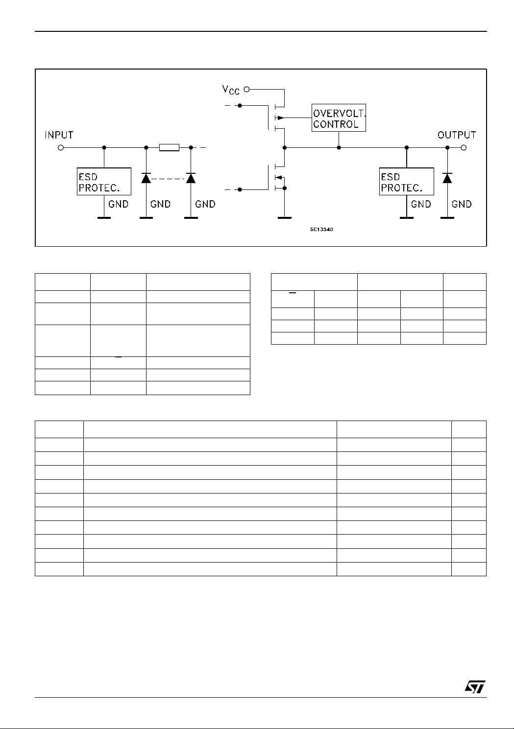
All inputs are equipped with protection circuits
against static discharge, giving them 2KV ESD
immunity and transient excess voltage.
All floating bus terminals during High Z State must
be held HIGH or LOW.
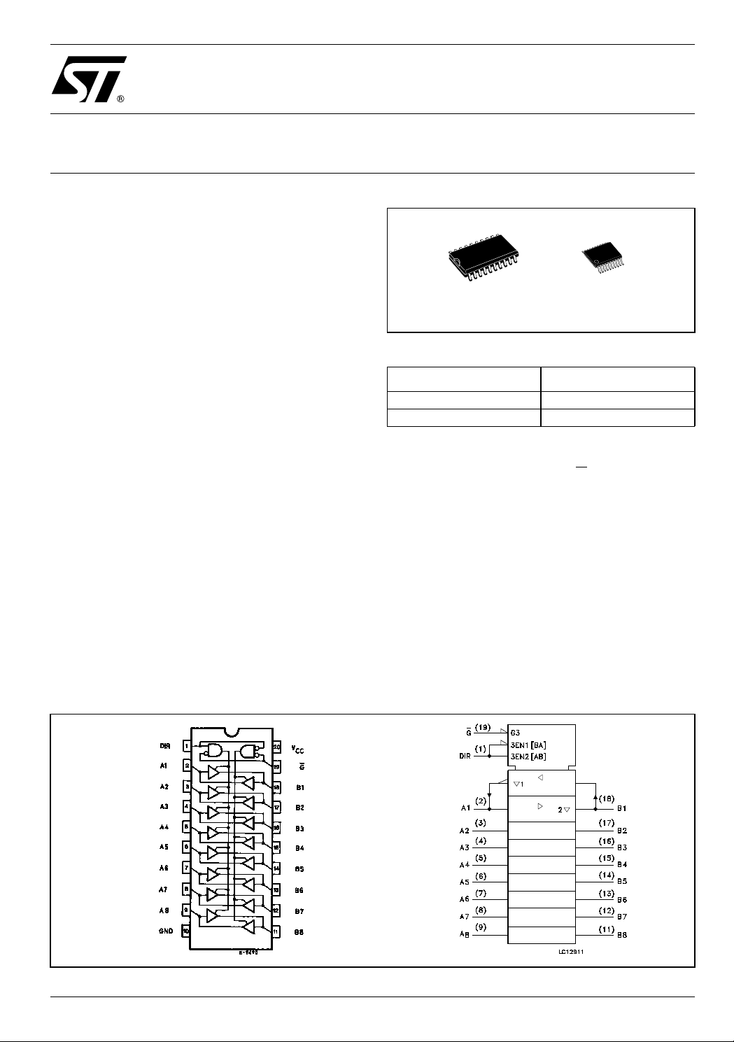
Figure 1: Pin C onnection And I EC Logic Symbol s
.
Rev. 4
1/12July 2004
74LVC245A
Figure 2: Input An d Output Equival e n t Ci rcui t
Table 2: Pin Description Table 3: Truth Table
PIN N° SYMBOL NAME AND FUNCTION
1 DIR Directional Control
2, 3, 4, 5, 6,
A1 to A8 Data Inputs/Outputs
7, 8, 9
18, 17, 16,
B1 to B8 Data Inputs/Outputs
15, 14, 13,
12, 11
19 G
Output Enable Input
INPUTS FUNCTION OUTPUT
G
DIR A BUS B BUS Yn
L L OUTPUT INPUT A = B
L H INPUT OUTPUT B = A
HXZZZ
X : Don’t Care
Z : High Impedance
10 GND Ground (0V)
20 V
CC
Positive Supply Voltage
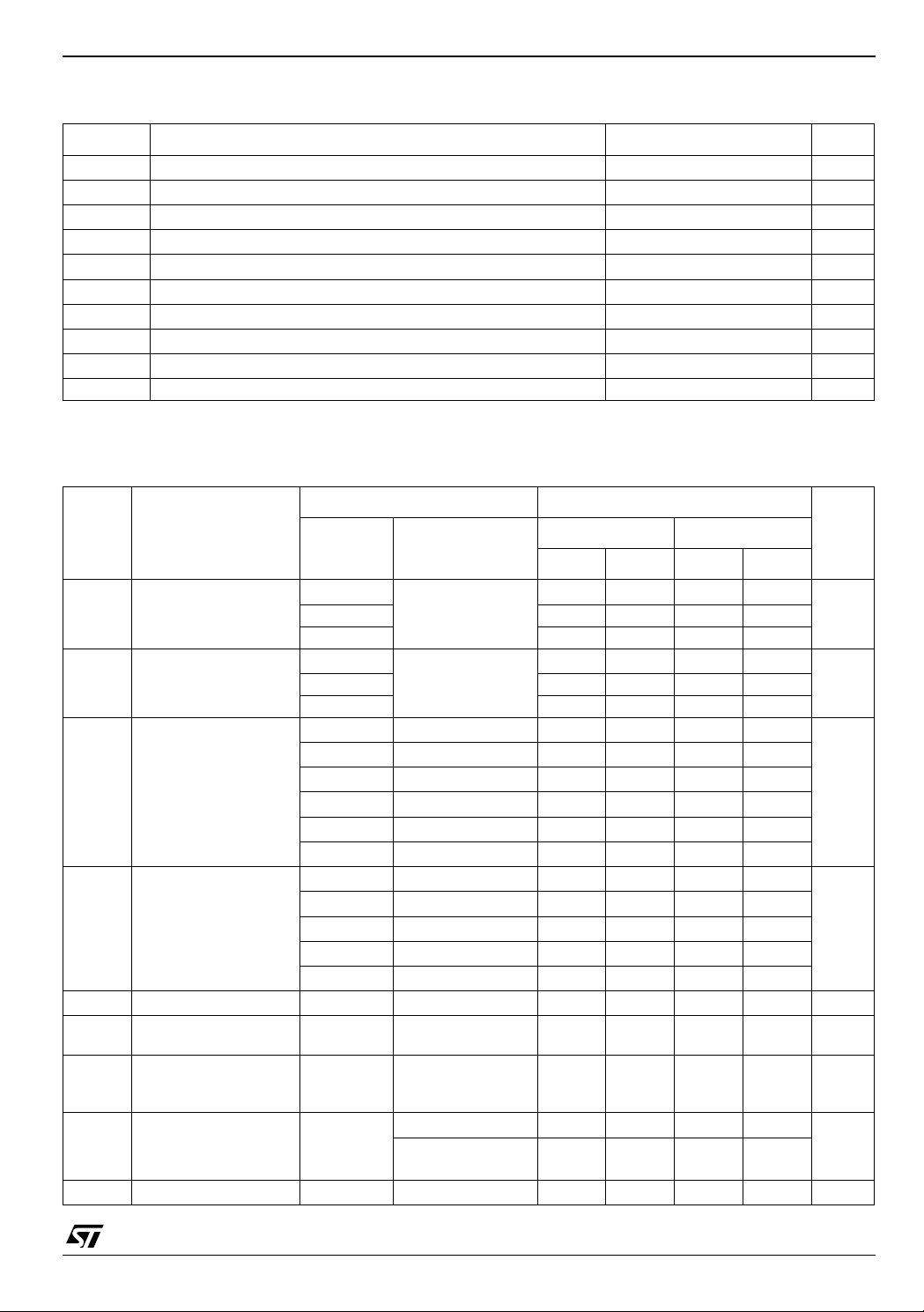
Table 4: Absolute Maximum Ratings
Symbol Parameter Value Unit
V
V
V
V
I
I
OK
I
or I
I
CC
T
T
Absolute Maximum Ratings are those values beyond which damage to the device may occur. Functional operation under these conditions is
not implied
1) IO absolute maximum rating must be observed
< GND
2) V
O
Supply Voltage
CC
DC Input Voltage
I
DC Output Voltage (High Impedance or VCC = 0V)
O
DC Output Voltage (High or Low State) (note 1) -0.5 to VCC + 0.5
O
DC Input Diode Current
IK
DC Output Diode Current (note 2)
DC Output Current
O
DC VCC or Ground Current per Supply Pin
GND
Storage Temperature
stg
Lead Temperature (10 sec)
L
-0.5 to +7.0 V
-0.5 to +7.0 V
-0.5 to +7.0 V
V
- 50 mA
- 50 mA
± 50 mA
± 100 mA
-65 to +150 °C
300 °C
2/12
74LVC245A
Table 5: Recommended Operating Conditions
Symbol Parameter Value Unit
V
V
V
V
I
OH
I
OH
I
OH
I
OH
T
dt/dv Input Rise and Fall Time (note 2) 0 to 10 ns/V
1) Truth T abl e guarante ed: 1.2V to 3.6V
2) VIN from 0.8V to 2V at VCC = 3.0V
Table 6: DC Specifications
Supply Voltage (note 1)
CC
Input Voltage
I
Output Voltage (High Impedance or VCC = 0V)
O
Output Voltage (High or Low State) 0 to V
O
, I
High or Low Level Output Current (VCC = 3.0 to 3.6V)
OL
, I
High or Low Level Output Current (VCC = 2.7 to 3.0V)
OL
, I
High or Low Level Output Current (VCC = 2.3 to 2.7V)
OL
, I
High or Low Level Output Current (VCC = 1.65 to 2.3V)
OL
Operating Temperature
op
Test Condition Value
1.65 to 3.6 V
0 to 5.5 V
0 to 5.5 V
CC
± 24 mA
± 12 mA
± 8mA
± 4mA
-55 to 125 °C
V
Symbol Parameter
High Level Input
V
IH
Voltage
V
Low Level Input
IL
Voltage
V
High Level Output
OH
Voltage
Low Level Output
V
OL
Voltage
Input Leakage Current
I
I
I
Power Off Leakage
off
Current
I
High Impedance
OZ
Output Leakage
Current
Quiescent Supply
I
CC
Current
∆I
CCICC
incr. per Input
V
CC
(V)
1.65 to 1.95
-40 to 85 °C -55 to 125 °C
Min. Max. Min. Max.
0.65V
CC
0.65V
CC
2.3 to 2.7 1.7 1.7
2.7 to 3.6 2 2
1.65 to 1.95
0.35V
CC
0.35V
2.3 to 2.7 0.7 0.7
2.7 to 3.6 0.8 0.8
1.65 to 3.6
1.65
2.3
2.7
3.0
3.0
1.65 to 3.6
1.65
2.3
2.7
3.0
3.6
0
3.6 V
3.6
2.7 to 3.6
IO=-100 µAVCC-0.2 VCC-0.2
=-4 mA
I
O
=-8 mA
I
O
=-12 mA
I
O
=-18 mA
I
O
I
=-24 mA
O
IO=100 µA
=4 mA
I
O
=8 mA
I
O
I
=12 mA
O
=24 mA
I
O
VI = 0 to 5.5V
or VO = 5.5V
V
I
= VIH orVIL
I
V
= 0 to 5.5V
O
VI = VCC or GND
V
or VO = 3.6 to
I
5.5V
VIH = VCC-0.6V
1.2 1.2
1.7 1.7
2.2 2.2
2.4 2.4
2.2 2.2
0.2 0.2
0.45 0.45
0.7 0.7
0.4 0.4
0.55 0.55
± 5 ± 5 µA
10 10 µA
± 10 ± 10 µA
10 10
± 10 ± 10
500 500 µA
Unit
V
CC
V
V
V
µA
3/12
74LVC245A
Table 7: Dynamic Switching Characteristics
Test Condition Value
= 25 °C
Symbol Parameter
V
CC
(V)
V
OLP
V
OLV
1) Number of output de fined as "n". M easured with "n -1" outputs switching fr om HI GH to LOW or LOW to HIGH. The rem ai ning output is
measur ed i n the LOW state.
Dynamic Low Level Quiet
Output (note 1)
3.3
= 50pF
C
L
V
= 0V, VIH = 3.3V
IL
Table 8: AC Electrical Characteristics
Test Condition Value
T
A
Min. Typ. Max.
0.8
-0.8
Unit
V
Symbol Parameter
t
PLH tPHL
Propagation Delay
Time
V
(V)
CC
C
(pF)
R
(Ω)
t
L
s
(ns)
L
1.65 to 1.95 30 1000 2.0 2.0 9.0 2.0 12
2.3 to 2.7 30 500 2.0 2.0 8.0 2.0 10.5
2.7 50 500 2.5 1.5 7.3 1.5 8.8
-40 to 85 °C -55 to 125 °C
= t
r
Min. Max. Min. Max.
Unit
ns
3.0 to 3.6 50 500 2.5 1.0 6.3 1.0 7.6
t
PZL tPZH
Output Enable Time 1.65 to 1.95 30 1000 2.0 2.0 12 2.0 16
2.3 to 2.7 30 500 2.0 2.0 9.5 2.0 12.5
2.7 50 500 2.5 1.0 9.0 1.0 11
ns
3.0 to 3.6 50 500 2.5 1.0 8.5 1.0 10
t
PLZ tPHZ
Output Disable Time 1.65 to 1.95 30 1000 2.0 2.0 11 2.0 14
2.3 to 2.7 30 500 2.0 2.0 9.0 2.0 12
2.7 50 500 2.5 2.0 8.5 2.0 10
ns
3.0 to 3.6 50 500 2.5 2.0 7.5 2.0 9.0
t
OSLH
t
OSHL
1) Skew is defined as the absolute value of the difference between the actual propagation delay for any two outputs of the same device switching in the sa me directio n, either HIGH or LOW (t
2) Param eter guaran teed by design
Output To Output
Skew Time (note1,
2)
2.7 to 3.6 1 1 ns
OSLH
= | t
PLHm
- t
PLHn
|, t
OSHL
= | t
PHLm
- t
PHLn
|
Table 9: Capacitive Characteristics
Test Condition Value
= 25 °C
Symbol Parameter
C
C
Input Capacitance
IN
Power Dissipation Capacitance
PD
(note 1)
V
CC
(V)
1.8 fIN = 10MHz 28
T
A
Min. Typ. Max.
4pF
Unit
pF2.5 30
3.3 34
1) CPD is defined as the value of the IC’s internal equivalent capacitance which is calculated from the operating current consumption without
load. (Refer to Test Circuit). Average operating current can be obtained by the following equation. I
= CPD x VCC x fIN + ICC/n (per c ircuit )
CC(opr)
4/12
 Loading...