

74LVC161284
LOW VOLTAG E HIGH SPEED IEEE1284 TRANSCEIVER
■ HIGH SPEED: t
■ LOW POWER DISSIPATION:
I
=20µA(MAX)atVCC=3.6V TA=85°C
CC
■ TTL COMPATIBLE INPUTS
V
=2V (MIN) VIL=0.8(MAX)
IH
■ OPERATING VOLTAGE RANGE:
V
(OPR) = 3.0V to 3.6V
CC
■ A PORT HAVE STANDARD 4mA TOTEM
= 9ns (MAX .) at VCC=3V
PD
POLE OUTPUT
■ B PORT HIGH DRIVE SOURCE/SINK
CAPABILITY OF 14mA
■ SUPPORTIEEE STD 1284-I (LEVEL 1 TYPE)
AND IEEE STD 1284-II (LEVEL 2 T YPE) FOR
BIDIRECTIONAL PARALLEL
COMMUNICATIONS BETWEEN PERSONAL
COMPUTER ANT PRINTING PERIPHERALS
■ TRANSLATION CAPABILITY ALLOW
OUTPUTSONCABLESIDETOINTERFACE
WITH 5 V SIGNAL
■ PULL-UP RESISTOR INTEGRATED ON ALL
OPEN-DRAIN OUTPUT ELIMINATE THE
NEED FOR DISCRETE RESISTOR
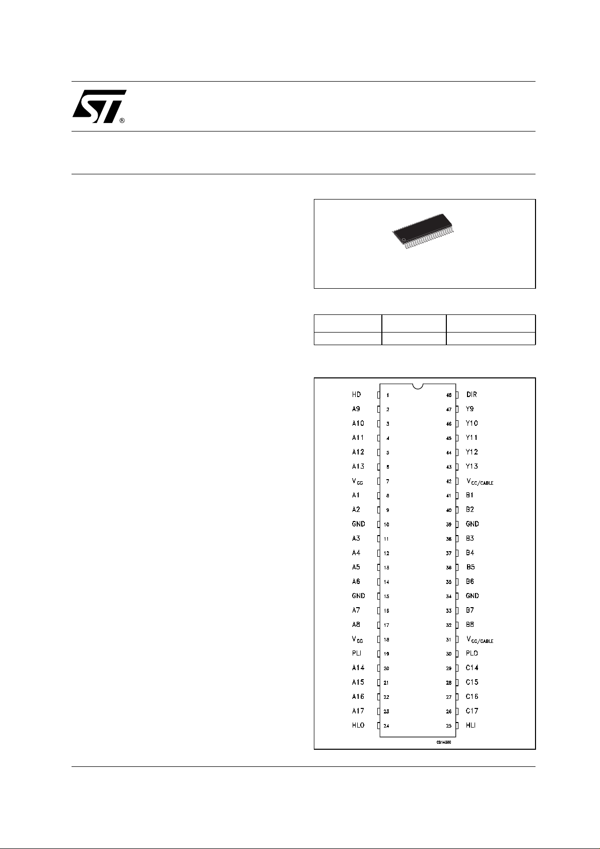
TSSOP
ORDER CODES
PACKAGE TUBE T & R
TSSOP 74LVC161284TTR
PIN CONNECTION
■ REPLACE THE FUNCTION OF TWO
74LVC1284 DEVICES
DESCRIPTION
The 74LVC161284 contains eight high speed non
inverting bidirectional buf fers and eleven control/
status non-inverting buffers with open drain
outputs fabricated in silicon gate C
2
MOS
technology. It’s intended to provide a standard
signaling m ethod for a bi-direction parallel
peripheral in an Extended Capabilities Port Mode
(ECP). The HD (Active HIGH) input pin enables
the Cable port to s witch from Open Drain to a high
drive tot em pole output, capable o f sourcing 14mA
on all thirteen buffer and 84mA on PERI LOGIC
OUTPUT buffer. The DIR input dete rmin es the
direction of data flow on the bidirectional buffers.
DIR (Active HIGH) enables data flow from A port
to B port. DIR (Active LOW) enables data flow
from B port to A port. It is available in the
commercial temperature range.
1/11May 2003
74LVC161284
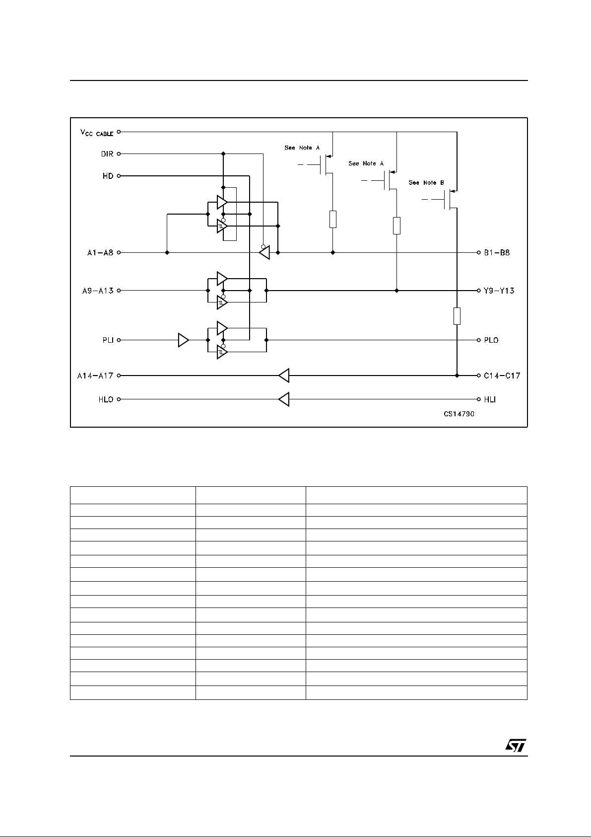
LOGIC DIAGRAM
NOTE A: The PMOS transistors prevent backdriving current from the signal pins to V
NOTE B: The PMOS transistor prevents backdriving current from the signal pins to V
PMOS transistor is turned off when the associated driver is in the low state.
CC/CABLE
CC/CABLE
when V
when V
PIN DESCRIPTION
PIN No SYMBOL NAME AND FUNCTION
1 HD High Drive Enable Input
2, 3, 4, 5, 6 A9 to A13 Side A Input
8, 9, 11, 12, 13, 14, 16, 17 A1 to A8 Side A Input or Output
19
20, 21, 22, 23 A14 to A17 Side A Output
24
25
29, 28, 27, 26 C14 to C17 Side Cable Output
30
41, 40, 38, 37, 36, 35, 33, 32 B1 to B8 Side Cable Input or Output
47, 46, 45, 44, 43 Y9 to Y13 Side Cable Output
48 DIR Direction Control Input
10, 15, 34, 39 GND Ground (0V)
7, 18
31, 42
PLI
HLO
HLI
PLO
V
CC
V
CC/CABLE
Peripheral Logic Input
Host Logic Output
Host Logic Input
Peripheral Logic Output
Positive Supply Voltage
Cable Power Supply
CC/CABLE
CC/CABLE
is open or at GND. The
is open or at GND.
2/11
TRUTH TABLE
74LVC161284
INPUT
OUTPUT OUTPUT
DIR HD
LL
B1-B8 Data to A1-A8
A9-A13 Data to Y9-Y13
LH
HL
C14-C17 Data to C14-C17
A1-A8 Data to B1-B8
A9-A13 Data to Y9-Y13
HH
C14-C17 Data to C14-C17
Y9-Y13 and PLO Open
Drain
Y9-Y13 and PLO Totem
Pole
B1-B8 Y9-Y13 and PLO
Open Drain
B1-B8 Y9-Y13 and PLO
Totem Pole
ABSOLUTE MAXIMUM RATINGS
Symbol Parameter Value Unit
V
V
CCcable
V
V
V
V
V
V
OBp
I
I
OK
I
or I
I
CC
T
T
Absolute Maximum Rating are those value beyond which damage to the device may occur. Functional operation under these condition is not
implied
Supply Voltage
CC
Cable Supply Voltage (must be ≥ VCC)
DC Input Voltage A1-A13, PLIN, DIR, HD
IA
DC Input Voltage B1-B8, C14-C17, HL
IB
DC Input Voltage B1-B8, C14-C17, HLIN(40ns transient)
IBp
DC Output Voltage A1-A8, A14-A17, HL
OA
DC Output Voltage B1-B8, Y9-Y13, PL
OB
IN
IN
IN
IN
DC Output Voltage B1-B8, Y9-Y13, PLIN(40ns transient)
DC Input Diode Current DIR, HD A9-A13, PLINC14-C17
IK
DC Output Diode Current A1-A8, A14-A17, HL
B1-B8, Y9-Y13, PL
DC Output Current A1-A8, HL
O
B1-B8, Y9-Y13 ± 50
PL
O
PL
O
DC VCCor Ground Current per Supply Pin
GND
Storage Temperature
stg
Lead Temperature (10 sec)
L
=LOW
= HIGH
-0.5 to +4.6 V
-0.5 to +7.0 V
-0.5to+VCC+0.5
V
-0.5 to +5.5 V
-2 to +7 V
-0.5to+VCC+0.5
V
-0.5 to +5.5 V
-2 to +7 V
-20 mA
IN
IN
IN
± 50 mA
-50
± 25 mA
84
-50
± 200 mA
-65 to +150 °C
300 °C
RECOMMENDED OPERATING CONDITIONS
Symbol Parameter Value Unit
V
V
CCcable
V
V
T
Supply Voltage
CC
Cable Supply Voltage
Input Voltage 0 to V
I
Open Drain Output Voltage
O
Operating Temperature
op
3.0 to 3.6 V
3.0 to 5.5 V
CC
0 to 5.5 V
-40 to 85 °C
V
3/11
74LVC161284
DC SPECIFICATIONS
Test Condition Value
Symbol Parameter
High Level
V
IH
Input Voltage
Low Level
V
IL
Input Voltage
V
High Level
OH
Output Voltage
An, Bn, PLIN, DIR, HD
HL
IN
An, Bn, PLIN, DIR, HD
HL
IN
An, HL
Bn, Yn 3.0 3.0
Bn, Yn 3.0 4.5
PL 3.15 3.15
V
Low Level
OL
Output Voltage
An, HL
Bn, Yn 3.0 3.0
Bn, Yn 3.0 4.5
PL 3.0 3.0
PL 3.0 4.5
I
Input Current Cn
I
All input except B or C
Quiescent Supply Current
I
CC
High
I
OZ
Impedance
Bn
Output
A1-A8
Open Drain Y Output
B, Y output (to GND)
B, Y output (to V
An, Bn, PLIN, DIR, HD
HL
IN
B1-B8, Y9-Y13 3.3 5.0
B1-B8, Y9-Y13,
C14-C17
I
OFF
V
Z
R
hys
O
P
Leakage
Current
Power Off
Leakage
Current
Input
Hysteresis
Output
Impedance
Pull-up
Resistance
CC
V
V
CC
(V)
3.0
3.6
3.0 3.0
3.0 3.0
3.0 3.0
3.0 3.0
3.6 3.6
3.6 3.6
3.6 5.0
3.6 5.0
3.6 5.0
3.6 3.6
3.6 5.0
3.6 3.6
)
CCcable
(V)
3.0
to
to
5.5
0 5.0
0 5.0
IO=-50µA
=-4mA
I
O
I
=-14mA
O
=-14mA
I
O
=-500µA
I
O
IO=50µA
=4mA
I
O
=14mA
I
O
=14mA
I
O
=84mA
I
O
=84mA
I
O
VI=V
=GND (Pull-up res)
V
I
V
I=VCC
or GND
VI=VCCIO=0
=GND (12xPull-up)
V
I
V
O=VCC
=GND (Pull-up res)
V
O
V
O=VCC
V
=GND (Pull-up res)
O
V
I
or GND
or VO=0to7V
VIor VO=0to7V
3.3 5.0 0.4
3.3 5.0 0.2
V
B=VOH
3.3 5.0
V
B=VOH
CC
-40 to 85 °C
Unit
Min. Max.
2
2.6
0.8
1.6
2.8
2.4
2.0
2.23
3.1
0.2
0.4
0.8
0.77
0.95
0.90
50 µA
-3.5 mA
± 1 µA
0.8
45
mA
20 µA
-3.5 mA
± 20 µA
-3.5 mA
100 µA
10 µA
30 55 Ω
1150 1650 Ω
VCn 2.3
VCn 0.8
V
V
VCn 3.3 5.0 0.8
4/11

AC ELECTRICAL CHARACTERISTICS
74LVC161284
Test Condition Value
Symbol Parameter
t
PLH
t
PHL
Propagation
Delay Time
A1-A8 to B1-B8,
A9-A13 to Y9-Y13
B1-B8 to A1-A8,
C14-C17 to A14-A17
PL
to PL
IN
OUT
to HL
HL
t
PZH
t
PZL
t
PLZ
t
PHZ
Enable Delay
Time
Disable Delay
Time
IN
DIR to A 3.0
HD to Bn, Y9-Y13
DIR to A
DIR to A R
OUT
HD to Bn, Y9-Y13 R
Rise and Fall Time
t
rtf
B1-B8, Y9-Y13 Open Drain
t
OSLH
t
OSHL
1) Skew is defined as the absolute value of the difference between the actual propagation delay for any two outputs of the same device
switching in the same direction, either HIGH or LOW (t
2) Parameter guaranteed by design
Output To Output Skew Time (note1, 2) 3.0
=|t
OSLH
V
CC
(V)
3.0
to
3.6
to
3.6
3.0
to
3.6
3.0
to
3.6
to
3.6
PLHm-tPLHn
V
CCcable
(V)
3.0
to
5.5
3.0
to
5.5
3.0
to
5.5
3.0
to
5.5
3.0
to
5.5
=500Ω CL=50pF
R
L
=500Ω CL=50pF
R
L
RL=500Ω CL=50pF
RL=500Ω CL=50pF
RL=500Ω CL=50pF
=500Ω CL=50pF
R
L
RL=500Ω CL=50pF
=500Ω CL=50pF
L
=500Ω CL=50pF
L
=500Ω CL=50pF
R
L
R
PULL-UP
|, t
=|t
OSHL
=500Ω
C
=50pF
L
PHLm-tPHLn
|
-40 to 85 °C
Unit
Min. Max.
1 7.5 ns
1 9.0 ns
1 7.0 ns
1 11.0 ns
112ns
1 8.5 ns
1 8.5 ns
1 8.5 ns
1 8.5 ns
1 120 ns
12ns
CAPACITANCE CHARACTERISTICS
Symbol Parameter
C
C
Control Input Capacitance
IN
(HD, DIR, A9-A13, C14-C17,
,HLIN)
PL
IN
I/O Pin Capacitance
I/O
Test Condition Value
V
(V)
CC
V
CC/CABLE
(V)
T
A
Min. Typ. Max.
Unit
=25°C
Open Open 4 pF
3.3 5.0 6 pF
5/11

74LVC161284
TEST CIRCUIT
TEST S1S2S3
t
(A1-A8 to B1-B8, A9-A13 to Y9-Y13, PLHINto PLH) (see waveform 1)
PHL
t
(A1-A8 to B1-B8, A9-A13 to Y9-Y13, PLHINto PLH, HD to B1-B8, Y9-Y13, PLH)
PLH
(see waveform 1)
t
PHL,tPLH
t
r,tf
t
PLZ
t
PHZ
t
PZL
t
PZH
t
PLZ
t
PHZ
CL= 50 pF or equivalent (includes jig and probe capacitance)
=R1=500Ω or equivalent
R
L
R
T=ZOUT
(B1-B8 to A1-A8, C14-C17 to A14-A17, HLHINto HLH) (see waveform 2)
(A1-A8 to B1-B8, A9-A13 to Y9-Y13) (see waveform 1)
(DIR to A1-A8) (see waveform 4) 6V GND GND
(DIR to A1-A8) (see waveform 4)
(DIR to A1-A8) (see waveform 3) 1.4V GND GND
(DIR to A1-A8) (see waveform 3) 4.4V GND GND
(DIR to B1-B8) (see waveform 4) 6V GND GND
(DIR to B1-B8) (see waveform 4)
of pulse generator (typically 50Ω)
Open
Open GND GND
Open
Open
Open
Open
V
CC
GND GND
V
CC
GND GND
GND GND
V
CC
GND
WAVEFORM 1: PROPAG ATION DE LAY INPUT An TO OUTPUT (f=1MHz; 50% d uty cycle)
6/11

74LVC161284
WAVEFORM 2: PROPAG ATION DE LAY INPUT Bn TO OUTPUT (f=1MHz; 50% d uty cycle)
VMO=50%V
CC
WAVEFORM 3: DATA T O OUTPUT ENABLE AND DISABLE TIME (f=1MHz; 50% duty cycle)
7/11

74LVC161284
WAVEFORM 4: DIR TO OUT PUT ENABLE AND DISABLE TIME (f=1MHz; 50% du ty cycle)
8/11

74LVC161284
TSSOP48 MECHANICAL DATA
mm. inch
DIM.
MIN. TYP MAX. MIN. TYP. MAX.
A 1.2 0.047
A1 0.05 0.15 0.002 0.006
A2 0.9 0.035
b 0.17 0.27 0.0067 0.011
c 0.09 0.20 0.0035 0.0079
D 12.4 12.6 0.488 0.496
E 8.1 BSC 0.318 BSC
E1 6.0 6.2 0.236 0.244
e 0 .5 BSC 0.0197 BSC
K0˚ 8˚0˚ 8˚
L 0.50 0.75 0.020 0.030
A2
A
A1
b
e
D
K
c
E1
L
E
PIN 1 IDENTIFICATION
1
7065588C
9/11

74LVC161284
Tape & Reel TSSOP48 MECHANICAL DATA
mm. inch
DIM.
MIN. TYP MAX. MIN. TYP. MAX.
A 330 12.992
C 12.8 13.2 0.504 0.519
D 20.2 0.795
N 60 2.362
T 30.4 1.197
Ao 8.7 8.9 0.343 0.350
Bo 13.1 13.3 0.516 0.524
Ko 1.5 1.7 0.059 0.067
Po 3.9 4.1 0.153 0.161
P 11.9 12.1 0.468 0.476
10/11

74LVC161284
Information furnished is believed to be accurate and reliable. However, STMicroelectronics assumes no responsibility for the
consequences of use o f suc h inf ormat ion n or f or an y infr ingeme nt of paten ts or oth er ri gh ts of third part ies whic h may resul t f rom
its use. No license is granted by implication or otherwise under any patent or patent rights of STMicroelectronics. Specifications
mentioned in this publication are subject to change without notice. This publication supersedes and replaces all information
previously supplied. STMicroelectronics products are not authorized for use as critical components in life support devices or
systems without express written approval of STMicroelectronics.
Australia - Brazil - Canada - China - Finland - France - Germany - Hong Kong - India - Israel - Italy - Japan - Malaysia - Malta - Morocco
© The ST logo is a registered trademark of STMicroelectronics
© 2003 STMicroelectronics - Printed in Italy - All Rights Reserved
STMicroelectronics GROUP OF COMPANIES
Singapore - Spain - Sweden - Switzerland - United Kingdom - United States.
© http://www.st.com
11/11
 Loading...