

ST 74LVC14A User Manual
74LVC14A
LOW VOLTAGE CMOS HEX INVERTER
HIGH PERFORMANCE
■ 5V TOLERANT INPUTS
■ HIGH SPEED: t
■ POWER DOWN PROTECTION ON INPUTS
= 5.0ns (MAX.) at VCC = 3V
PD
AND OUTPUTS
■ SYMMETRICAL OUTPUT IMPEDANCE:
|I
| = IOL = 24mA (MIN) at VCC = 3V
OH
■ PCI BUS LEVELS GUARANTEED AT 24 mA
■ BALANCED PROPAGATION DELAYS:
t
≅ t
PLH
■ OPERATING VOLTAGE RANGE:
V
CC
PHL
(OPR) = 1.65V to 3.6V (1.2V Data
Retention)
■ PIN AND FUNCTION COMPATIBLE WITH
74 SERIES 00
■ LA TCH-UP PERFORMANCE EXCEEDS
500mA (JESD 17)
■ ESD PERFORMANCE:
HBM > 2000V (MIL STD 883 method 3015);
MM > 200V
DESCRIPTION
The 74LVC14A is a low voltage CMOS HEX
SCHMITT INVERTER fabricated with sub-micron
silicon gate and double-layer metal wiring C
technology. It is ideal for 1.65 to 3.6 V
2
MOS
CC
operations and low power and low noise
applications.
TSSOPSOP
Table 1: Order Codes
PACKAGE T & R
SOP 74LVC14AMTR
TSSOP 74LVC14ATTR
It can be interfaced to 5V signal environment for
inputs in mixed 3.3/5V system.
It has more sp eed performance at 3.3V than 5V
AC/ACT family, combined with a lower power
consumption.
Pin configuration and function are the same as
those of the 74LVC04A but the 74LVC14A has
hysteresis between the positive and negative
input threshold typically of 700mV.
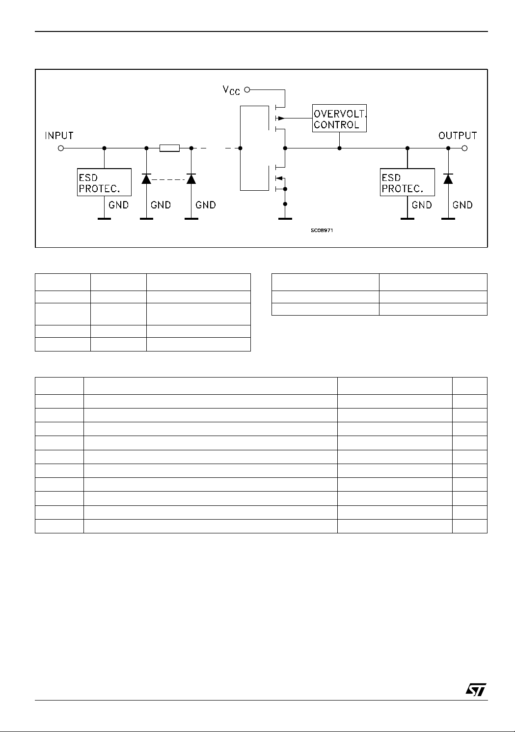
All inputs and outputs are equipped with
protection circuits against static disc harge, giving
them 2KV ESD immunity and transient excess
voltage.
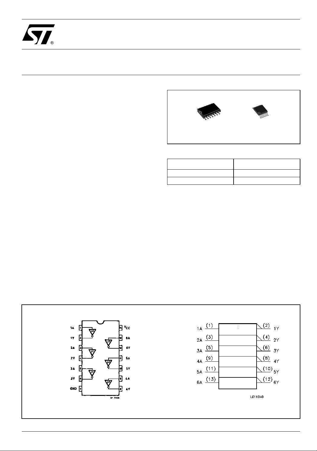
Figure 1: Pin C onnection And I EC Logic Symbol s
Rev. 7
1/12July 2004
74LVC14A
Figure 2: Input An d Output Equival e n t Ci rcui t
Table 2: Pin Description Table 3: Truth Table
PIN N° SYMBOL NAME AND FUNCTION
1,3,5,9,11,13 1A to 6A Data Inputs
2, 4, 6, 8,
10, 12
1Y to 6Y Data Outputs
AY
LH
HL
7 GND Ground (0V)
14
V
CC
Positive Supply Voltage
Table 4: Absolute Maximum Ratings
Symbol Parameter Value Unit
V
V
V
V
I
I
OK
I
or I
I
CC
T
T
Absolute Maximum Ratings are those values beyond which damage to the device may occur. Functional operation under these conditions is
not implied
1) IO absolute maximum rating must be observed
< GND
2) V
O
Supply Voltage
CC
DC Input Voltage
I
DC Output Voltage (VCC = 0V)
O
DC Output Voltage (High or Low State) (note 1) -0.5 to VCC + 0.5
O
DC Input Diode Current
IK
DC Output Diode Current (note 2)
DC Output Current
O
DC VCC or Ground Current per Supply Pin
GND
Storage Temperature
stg
Lead Temperature (10 sec)
L
-0.5 to +7.0 V
-0.5 to +7.0 V
-0.5 to +7.0 V
V
- 50 mA
- 50 mA
± 50 mA
± 100 mA
-65 to +150 °C
300 °C
2/12
74LVC14A
Table 5: Recommended Operating Conditions
Symbol Parameter Value Unit
V
V
V
V
I
OH
I
OH
I
OH
I
OH
T
dt/dv Input Rise and Fall Time (note 2) 0 to 10 ns/V
1) Truth T abl e guarante ed: 1.2V to 3.6V
from 0.8V to 2V at VCC = 3.0V
2) V
IN
Supply Voltage (note 1)
CC
Input Voltage
I
Output Voltage (VCC = 0V)
O
Output Voltage (High or Low State) 0 to V
O
, I
High or Low Level Output Current (VCC = 3.0 to 3.6V)
OL
, I
High or Low Level Output Current (VCC = 2.7 to 3.0V)
OL
, I
High or Low Level Output Current (VCC = 2.3 to 2.7V)
OL
, I
High or Low Level Output Current (VCC = 1.65 to 2.3V)
OL
Operating Temperature
op
1.65 to 3.6 V
0 to 5.5 V
0 to 5.5 V
CC
± 24 mA
± 12 mA
± 8mA
± 4mA
-55 to 125 °C
V
3/12
74LVC14A
Table 6: DC Specifications
Test Condition Value
Symbol Parameter
V
V
V
V
V
I
I
CC
∆I
Positive Input
T+
threshold
Negative Input
T-
threshold
Hysteresis Voltage 1.65 to 1.95 0.3 1.1 0.3 1.1
H
High Level Output
OH
Voltage
Low Level Output
OL
Voltage
Input Leakage
I
I
Current
Power Off Leakage
off
Current
Quiescent Supply
Current
ICC incr. per Input
CC
V
CC
(V)
-40 to 85 °C -55 to 125 °C
Min. Max. Min. Max.
1.65 to 1.95 0.6 1.4 0.6 1.4
2.3 to 2.7 0.8 2.0 0.8 2.0
3.0 0.8 2.0 0.8 2.0
3.6 0.8 2.2 0.8 2.2
1.65 to 1.95 0.3 1.0 0.3 1.0
2.3 to 2.7 0.4 1.4 0.4 1.4
3.0 0.6 1.5 0.6 1.5
3.6 0.8 1.8 0.8 1.8
2.3 to 2.7 0.3 1.1 0.3 1.1
3.0 0.3 1.2 0.3 1.2
3.6 0.3 1.2 0.3 1.2
1.65 to 3.6
1.65
2.3
2.7
3.0
3.0
1.65 to 3.6
1.65
2.3
2.7
3.0
3.6
0
3.6
2.7 to 3.6
IO=-100 µAVCC-0.2 VCC-0.2
=-4 mA
I
O
=-8 mA
I
O
=-12 mA
I
O
I
=-12 mA
O
=-24 mA
I
O
=100 µA
I
O
=4 mA
I
O
I
=8 mA
O
=12 mA
I
O
=24 mA
I
O
V
= 0 to 5.5V
I
or VO = 5.5V
V
I
VI = VCC or GND
or VO = 3.6 to
V
I
5.5V
VIH = VCC-0.6V
1.2 1.2
1.7 1.7
2.2 2.2
2.4 2.4
2.2 2.2
0.2 0.2
0.45 0.45
0.7 0.7
0.4 0.4
0.55 0.55
± 5 ± 5 µA
10 10 µA
10 10
± 10 ± 10
500 500 µA
Unit
V
V
V
V
µA
Table 7: Dynamic Switching Characteristics
Test Condition Value
= 25 °C
Symbol Parameter
V
CC
(V)
V
OLP
V
OLV
1) Number of output de fined as "n". M easured with "n -1" outputs switching fr om HI GH to LOW or LOW to HIGH. The rem ai ning output is
measur ed i n the LOW state.
Dynamic Low Level Quiet
Output (note 1)
3.3
= 50pF
C
L
V
= 0V, VIH = 3.3V
IL
4/12
T
A
Min. Typ. Max.
0.8
-0.8
Unit
V
 Loading...