

ST 74LCX74 User Manual
Low voltage CMOS dual D-Type Flip Flop
Features
■ 5V tolerant inputs
■ High speed:
–f
■ Power down protection on inputs and outputs
■ Symmetrical output impedance:
–|I
■ PCI bus levels guaranteed at 24mA
■ Balanced propagation delays:
–t
■
Operating voltage range:
–V
■ Pin and function compatible with
74 series 74
■ Latch-up performance exceeds
500mA (JESD 17)
■ ESD performance:
– HBM > 2000V
= 150MHz (Max) at V
MAX
| = IOL = 24mA (Min) at VCC = 3V
OH
≅ t
PLH
PHL
(Opr) = 2.0V to 3.6V
CC
CC
= 3V
(MIL STD 883 method 3015); MM > 200V
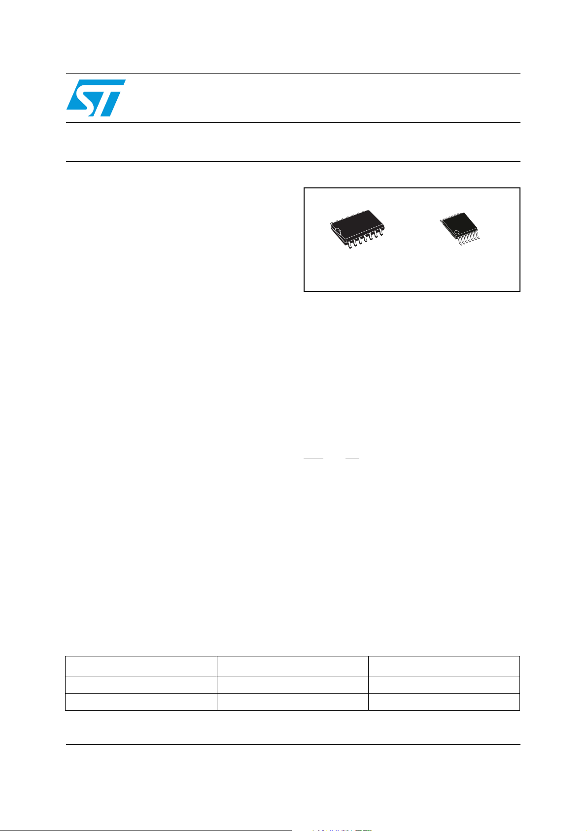
74LCX74
with 5V tolerant inputs
SO-14 TSSOP14
Description
The 74LCX74 is a low voltage CMOS dual D-type
flip flop with preset and clear non inverting
fabricated with sub-micron silicon gate and
double-layer metal wiring C
ideal for low power and high speed 3.3V
applications; it can be interfaced to 5V signal
environment for inputs.
A signal on the D INPUT is transferred to the Q
OUTPUT during the positive going transition of
the clock pulse.
CLR
and PR are independent of the clock and
accomplished by a low setting on the appropriate
input.
2
MOS technology. It is
It has same speed performance at 3.3V than 5V
AC/ACT family, combined with a lower power
consumption.
All inputs and outputs are equipped with
protection circuits against static discharge, giving
them 2KV ESD immunity and transient excess
voltage.
Order codes
Part number Package Packaging
74LCX74MTR SO-14 Tape and reel
74LCX74TTR TSSOP14 Tape and reel
July 2006 Rev 8 1/17
www.st.com
17

Contents 74LCX74
Contents
1 Logic symbols and I/O equivalent circuit . . . . . . . . . . . . . . . . . . . . . . . . 3
1.1 Logic diagram . . . . . . . . . . . . . . . . . . . . . . . . . . . . . . . . . . . . . . . . . . . . . . . 3
2 Pin settings . . . . . . . . . . . . . . . . . . . . . . . . . . . . . . . . . . . . . . . . . . . . . . . . 4
2.1 Pin connection . . . . . . . . . . . . . . . . . . . . . . . . . . . . . . . . . . . . . . . . . . . . . . 4
2.2 Pin description . . . . . . . . . . . . . . . . . . . . . . . . . . . . . . . . . . . . . . . . . . . . . . 4
2.3 Truth table . . . . . . . . . . . . . . . . . . . . . . . . . . . . . . . . . . . . . . . . . . . . . . . . . . 4
3 Maximum rating . . . . . . . . . . . . . . . . . . . . . . . . . . . . . . . . . . . . . . . . . . . . . 5
3.1 Recommended operating conditions . . . . . . . . . . . . . . . . . . . . . . . . . . . . . 5
4 Electrical characteristics . . . . . . . . . . . . . . . . . . . . . . . . . . . . . . . . . . . . . 6
5 Test circuit . . . . . . . . . . . . . . . . . . . . . . . . . . . . . . . . . . . . . . . . . . . . . . . . . 8
6 Waveforms . . . . . . . . . . . . . . . . . . . . . . . . . . . . . . . . . . . . . . . . . . . . . . . . . 8
7 Package mechanical data . . . . . . . . . . . . . . . . . . . . . . . . . . . . . . . . . . . . 11
8 Revision history . . . . . . . . . . . . . . . . . . . . . . . . . . . . . . . . . . . . . . . . . . . 16
2/17
74LCX74 Logic symbols and I/O equivalent circuit
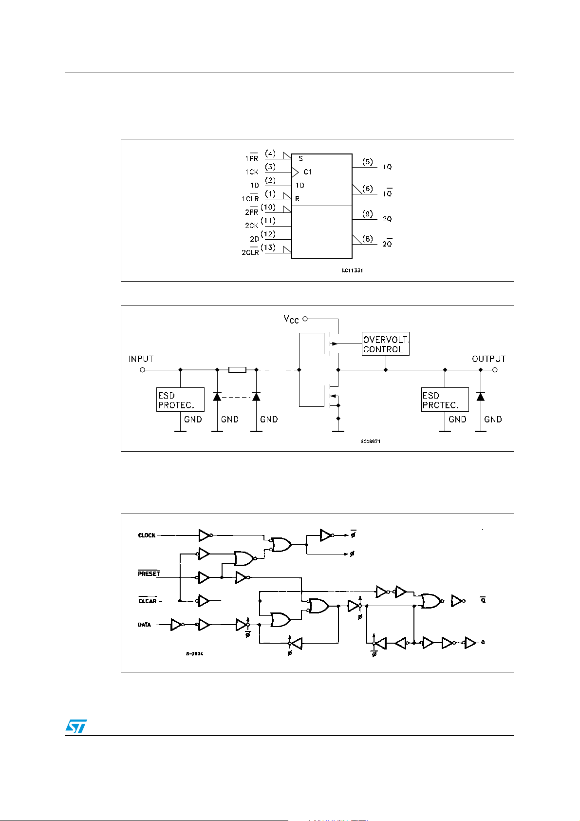
1 Logic symbols and I/O equivalent circuit
Figure 1. IEC logic symbols
Figure 2. Input and output equivalent circuit
1.1 Logic diagram
Figure 3. Logic diagram
Note: This logic diagram has not to be used to estimate propagation delays
3/17
Pin settings 74LCX74
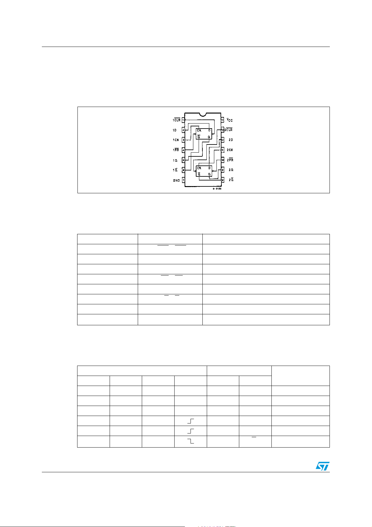
2 Pin settings
2.1 Pin connection
Figure 4. Pin connection (top through view)
2.2 Pin description
Table 1. Pin description
Pin N° Symbol Name and function
1, 13 1CLR, 2CLR Asynchronous reset - direct input
2, 12 1D, 2D Data inputs
3, 11 1CK, 2CK Clock input (LOW to HIGH, Edge Triggered)
4, 10 1PR
5, 9 1Q, 2Q True Flip-Flop outputs
6, 8 1Q
7 GND Ground (0V)
14 V
2.3 Truth table
Table 2. Truth table
CLR PR D CK Q Q
L H X X L H CLEAR
H L X X H L PRESET
LLXXHH
HHL LH
HHH HL
HH
1. X do not care
, 2PR Asynchronous set - direct input
, 2Q Complement Flip-Flop outputs
CC
Inputs Outputs
(1)
X
Positive supply voltage
Q
n
Function
Q
n
No change
4/17
74LCX74 Maximum rating
3 Maximum rating
stressing the device above the rating listed in the “absolute maximum ratings” table may
cause permanent damage to the device. these are stress ratings only and operation of the
device at these or any other conditions above those indicated in the operating sections of
this specification is not implied. exposure to absolute maximum rating conditions for
extended periods may affect device reliability. refer also to the STMicroelectronics sure
program and other relevant quality documents.
Table 3. Absolute maximum ratings
Symbol Parameter Value Unit
V
I
I
I
GND
T
1. IO absolute maximum rating must be observed
2. VO < GND
Supply voltage -0.5 to +7.0 V
CC
V
DC input voltage -0.5 to +7.0 V
I
DC output voltage (VCC = 0V)
V
O
V
DC output voltage (high or low state)
O
I
DC input diode current -50 mA
IK
DC output diode current
OK
I
DC output current ± 50 mA
O
DC supply current per supply pin ± 100 mA
CC
(2)
(1)
-0.5 to +7.0 V
-0.5 to VCC + 0.5
-50 mA
DC ground current per supply pin ± 100 mA
Storage temperature -65 to +150 °C
stg
T
Lead temperature (10 sec) 300 °C
L
V
3.1 Recommended operating conditions
Table 4. Recommended operating conditions
Symbol Parameter Value Unit
V
V
V
V
Supply voltage
CC
Input voltage 0 to 5.5 V
I
Output voltage (VCC = 0V)
O
Output voltage (high or low state)
O
IOH, IOLHigh or low level output current (VCC = 3.0 to 3.6V)
I
, IOLHigh or low level output current (VCC = 2.7V)
OH
T
dt/dv
1. Truth table guaranteed: 1.5V to 3.6V
2. VIN from 0.8V to 2V at VCC = 3.0V
Operating temperature -40 to 85 °C
op
Input Rise and Fall Time
(1)
(2)
5/17
2.0 to 3.6 V
0 to 5.5 V
0 to V
CC
± 24 mA
± 12 mA
0 to 10 ns/V
V
Electrical characteristics 74LCX74
4 Electrical characteristics
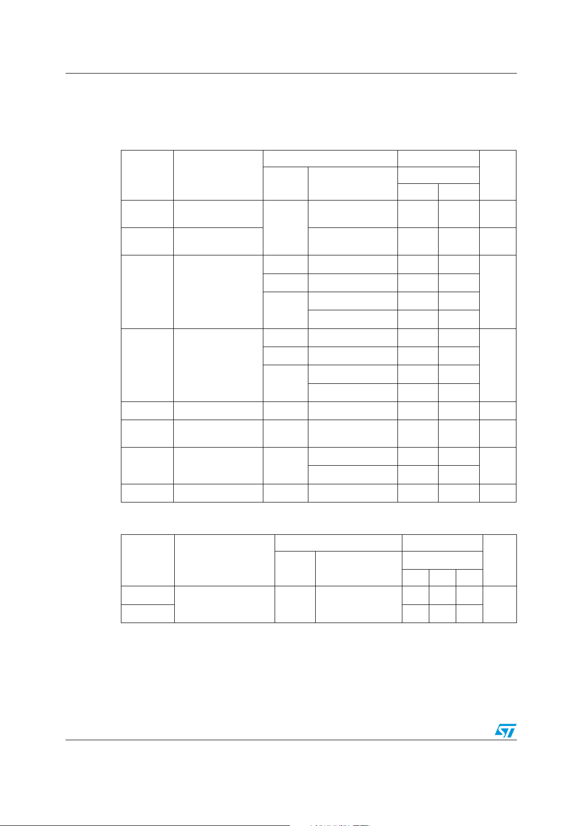
Table 5. DC specifications
Test condition Value
Symbol Parameter
V
CC
(V)
-40 to 85°C
Min Max
Unit
V
IH
High level input
voltage
2.0 V
2.7 to 3.6
V
V
OH
V
OL
I
I
off
I
CC
∆I
CC
Low level input
IL
voltage
High level output
voltage
Low level output
voltage
Input leakage current 2.7 to 3.6
I
Power OFF leakage
current
Quiescent supply
current
I incr. per Input 2.7 to 3.6
2.7 to 3.6
2.7
3.0
2.7 to 3.6
2.7
3.0
0
2.7 to 3.6
=-100 µAVCC-0.2
I
O
=-12 mA
I
O
I
=-18 mA
O
I
=-24 mA
O
I
=100 µA
O
=12 mA
I
O
I
=16 mA
O
I
=24 mA
O
= 0 to 5.5V
V
I
VI or VO = 5.5V
VI = VCC or GND
V
or VO= 3.6 to 5.5V
I
= VCC - 0.6V
V
IH
0.8 V
2.2
V
2.4
2.2
0.2
0.4
V
0.4
0.55
± 5 µA
10 µA
10
µA
± 10
500 µA
Table 6. Dynamic switching characteristics
Symbol Parameter
V
OLP
V
OLV
1. Number of outputs defined as "n". Measured with "n-1" outputs switching from HIGH to LOW or LOW to
HIGH. The remaining output is measured in the LOW state.
Dynamic low level quiet
(1)
output
6/17
V
Test condition Value
CC
(V)
= 50pF
C
3.3
L
VIL = 0V, VIH = 3.3V
TA = 25 °C
Min Typ Max
0.8
-0.8
Unit
V
 Loading...