

ST 74LCX573 User Manual
74LCX573
OCTAL D-TYPE LATCH NON-INVERTING (3-STATE)
WITH 5V TOLERANT INPUTS AND OUTPUTS
■ 5V TOLERANT INPUTS AND OUTPUTS
■ HIGH SPEED:
t
= 8.0 ns (MAX.) at VCC = 3V
PD
■ POWER DOWN PROTECTION ON INPUTS
AND OUTPUTS
■ SYMMETRICAL OUTPUT IMPEDANCE:
| = IOL = 24mA (MIN) at VCC = 3V
|I
OH
■ PCI BUS LEVELS GUARANTEED AT 24 mA
■ BALANCED PROPAGATION DELAYS:
t
≅ t
PLH
■ OPERATING VOLTAGE RANGE:
V
CC
PHL
(OPR) = 2.0V to 3.6V (1.5V Data
Retention)
■ PIN AND FUNCTION COMPATIBLE WITH
74 SERIES 573
■ LA TCH-UP PERFORMANCE EXCEEDS
500mA (JESD 17)
■ ESD PERFORMANCE:
HBM > 2000V (MIL STD 883 method 3015);
MM > 200V
DESCRIPTION
The 74LCX573 is a low voltage CMOS OCTAL
D-TYPE LATCH with 3 STATE OUTPUT
NON-INVERTING fabricated with sub-micron
silicon gate and double-layer metal wiring C
2
MOS
technology. It is ideal for low power and high
speed 3.3V applications; it can be interfaced to 5V
signal environment for both inputs and outputs.
These 8 bit D-Type latch are controlled by a latch
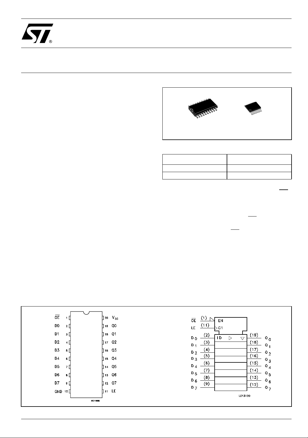
Figure 1: Pin C onnection And I EC Logic Symbol s
TSSOPSOP
Table 1: Order Codes
PACKAGE T & R
SOP 74LCX573MTR
TSSOP 74LCX573TTR
enable input (LE) and an output enable input (OE
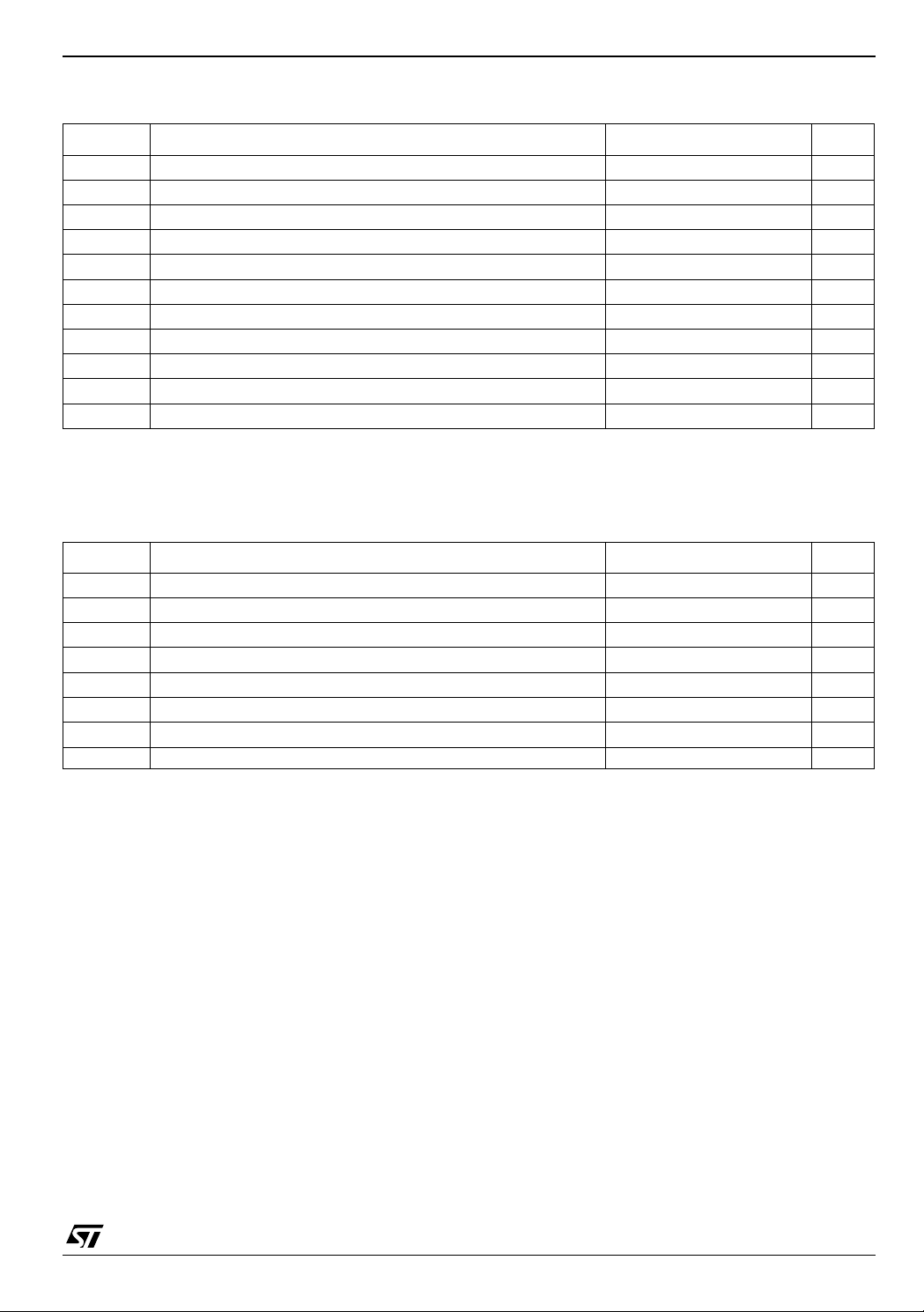
While the LE inputs is held a t a high level, the Q
outputs will follow the data input . When the LE is
taken low, the Q outputs will be latched at the logic
lev el of D inp ut d ata. W hile the (OE
) input is low,
the 8 outputs will be in a normal logic state (high or
low logic level) and while (OE
) is in hig h le v el, the
outputs will be in a high impedance state.
It has same speed performance at 3.3V than 5V
AC/ACT family, combined with a lower power
consumption.
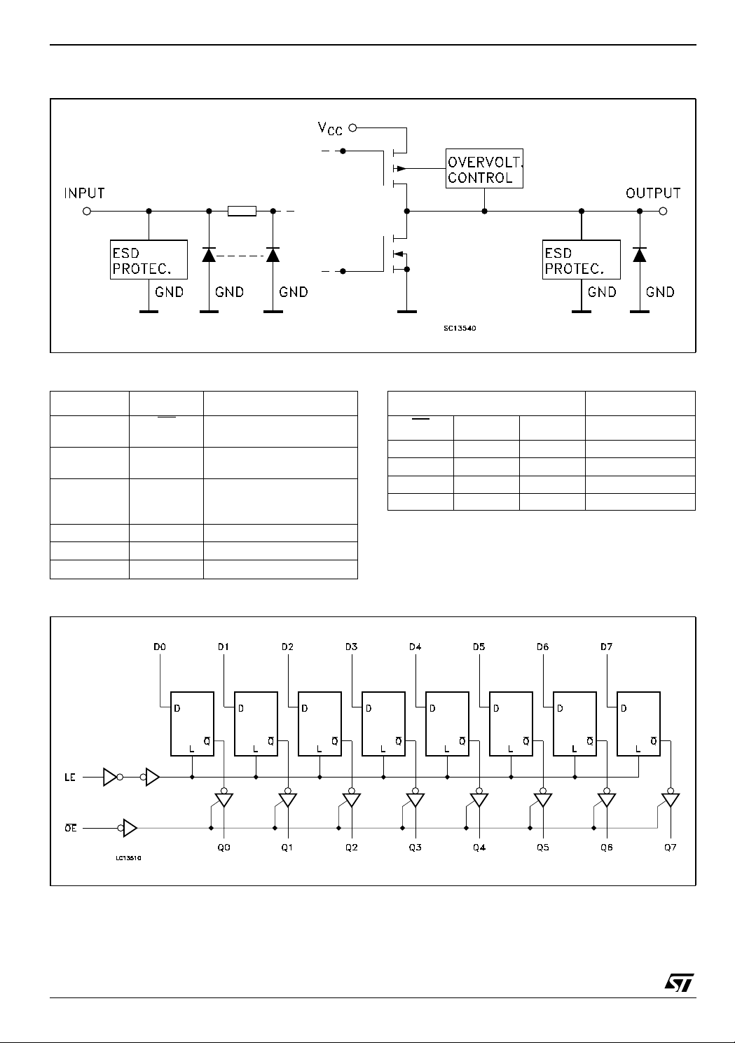
All inputs and outputs are equipped with
protection circuits against static disc harge, giving
them 2KV ESD immunity and transient excess
voltage.
).
Rev. 5
1/13September 2004
74LCX573
Figure 2: Input An d Output Equival e n t Ci rcui t
Table 2: Pin Description Table 3: Truth Table
PIN N° SYMBOL NAME AND FUNCTION
1OE3 State Output Enable
Input (Active LOW)
2, 3, 4, 5, 6,
D0 to D7 Data Inputs
7, 8, 9
12, 13, 14,
Q0 to Q7 3-State Latch Outputs
15, 16, 17,
18, 19
11 LE Latch Enable Input
10 GND Ground (0V)
20 V
CC
Positive Supply Voltage
Figure 3: Logic Diagram
INPUT OUTPUT
OE
LE D Q
HXX Z
L L X NO CHANGE*
LHL L
LHH H
X : Don’t Care
Z : High Impedance
* : Q Outputs are latched at the time when th e LE i nput is taken
LOW.
This logi c di agram has not be used to estim ate propaga tion delays
2/13
74LCX573
Table 4: Absolute Maximum Ratings
Symbol Parameter Value Unit
V
V
V
V
I
I
OK
I
I
CC
I
GND
T
T
Absolute Maximum Ratings are those values beyond which damage to the device may occur. Functional operation under these conditions is
not implied
absolute maximum rating must be observed
1) I
O
< GND
2) V
O
Table 5: Recommended Operating Conditions
Supply Voltage
CC
DC Input Voltage
I
DC Output Voltage (OFF State)
O
DC Output Voltage (High or Low State) (note 1) -0.5 to VCC + 0.5
O
DC Input Diode Current
IK
DC Output Diode Current (note 2)
DC Output Current
O
DC Supply Current per Supply Pin
DC Ground Current per Supply Pin
Storage Temperature
stg
Lead Temperature (10 sec)
L
-0.5 to +7.0 V
-0.5 to +7.0 V
-0.5 to +7.0 V
V
- 50 mA
- 50 mA
± 50 mA
± 100 mA
± 100 mA
-65 to +150 °C
300 °C
Symbol Parameter Value Unit
I
I
V
V
V
V
OH
OH
T
Supply Voltage (note 1)
CC
Input Voltage
I
Output Voltage (OFF State)
O
Output Voltage (High or Low State) 0 to V
O
, I
High or Low Level Output Current (VCC = 3.0 to 3.6V)
OL
, I
High or Low Level Output Current (VCC = 2.7V)
OL
Operating Temperature
op
2.0 to 3.6 V
0 to 5.5 V
0 to 5.5 V
CC
± 24 mA
± 12 mA
-55 to 125 °C
dt/dv Input Rise and Fall Time (note 2) 0 to 10 ns/V
1) Truth T abl e guarante ed: 1.5V to 3.6V
from 0.8V to 2V at VCC = 3.0V
2) V
IN
V
3/13
74LCX573
Table 6: DC Specifications
Test Condition Value
Symbol Parameter
V
V
V
V
I
I
OZ
High Level Input
IH
Voltage
Low Level Input
IL
Voltage
High Level Output
OH
Voltage
Low Level Output
OL
Voltage
Input Leakage
I
I
Current
Power Off Leakage
off
Current
High Impedance
Output Leakage
Current
I
CC
∆I
Quiescent Supply
Current
ICC incr. per Input
CC
V
CC
(V)
2.7 to 3.6
2.7 to 3.6
2.7
3.0
2.7 to 3.6
2.7
3.0
2.7 to 3.6
0
2.7 to 3.6
2.7 to 3.6
2.7 to 3.6
-40 to 85 °C -55 to 125 °C
Min. Max. Min. Max.
2.0 2.0 V
0.8 0.8 V
IO=-100 µAVCC-0.2 VCC-0.2
I
=-12 mA
O
=-18 mA
I
O
=-24 mA
I
O
IO=100 µA
I
=12 mA
O
I
=16 mA
O
=24 mA
I
O
= 0 to 5.5V
V
I
or VO = 5.5V
V
I
= VIH or V
V
I
VO = 0 to V
VI = VCC or GND
V
or VO= 3.6 to 5.5V
I
VIH = VCC - 0.6V
IL
CC
2.2 2.2
2.4 2.4
2.2 2.2
0.2 0.2
0.4 0.4
0.4 0.4
0.55 0.55
± 5 ± 5 µA
10 10 µA
± 5 ± 5 µA
10 10
± 10 ± 10
500 500 µA
Unit
V
V
µA
Table 7: Dynamic Switching Characteristics
Test Condition Value
= 25 °C
Symbol Parameter
V
CC
(V)
V
OLP
V
OLV
1) Number of outputs defined as "n". Measured wi t h "n-1" output s switching from HIGH to LO W or LOW to HIGH. The remaining output is
measur ed i n the LOW state.
Dynamic Low Level Quiet
Output (note 1)
3.3
= 50pF
C
L
V
= 0V, VIH = 3.3V
IL
T
A
Min. Typ. Max.
0.8
-0.8
Unit
V
4/13
 Loading...