

ST 74LCX245 User Manual
74LCX245
LOW VOLTAGE CMOS OCTAL BUS TRANSCEIVER
(3-STATE) WITH 5V TO LER A N T IN PU TS AN D OUTPUTS
■ 5V TOLERANT INPUTS AND OUTPUTS
■ HIGH SPEED:
t
= 7.0 ns (MAX.) at VCC = 3V
PD
■ POWER DOWN PROTECTION ON INPUTS
AND OUTPUTS
■ SYMMETRICAL OUTPUT IMPEDANCE:
|I
| = IOL = 24mA (MIN) at VCC = 3V
OH
■ PCI BUS LEVELS GUARANTEED AT 24 mA
■ BALANCED PROPAGATION DELAYS:
t
≅ t
PLH
PHL
■ OPERATING VOLTAGE RANGE:
V
(OPR) = 2.0V to 3.6V (1.5V Data
CC
Retention)
■ PIN AND FUNCTION COMPATIBLE WITH
74 SERIES 245
■ LA TCH-UP PERFORMANCE EXCEEDS
500mA (JESD 17)
■ ESD PERFORMANCE:
HBM > 2000V (MIL STD 883 method 3015);
MM > 200V
DESCRIPTION
The 74LCX245 is a low voltage CMOS OCTAL
BUS TRANSCEIVER (3-STATE) fabricated with
sub-micron silicon gate and double-layer metal
wiring C
2
MOS technology. It is ideal for low power
and high speed 3.3V applications; it can be
interfaced to 5V signal environment for both inputs
and ou tputs.
TSSOPSOP
Table 1: Order Codes
PACKAGE T & R
SOP 74LCX245MTR
TSSOP 74LCX245TTR
It has same speed performance at 3.3V than 5V
AC/ACT family, combined with a lower power
consumption.
This IC is intended for two way asynchronous
communication betwee n data bu ses; the direction
of data transmission is determined by DIR input.
The enable input G
can be used to disable the
device so that the buses are effectively isolated.
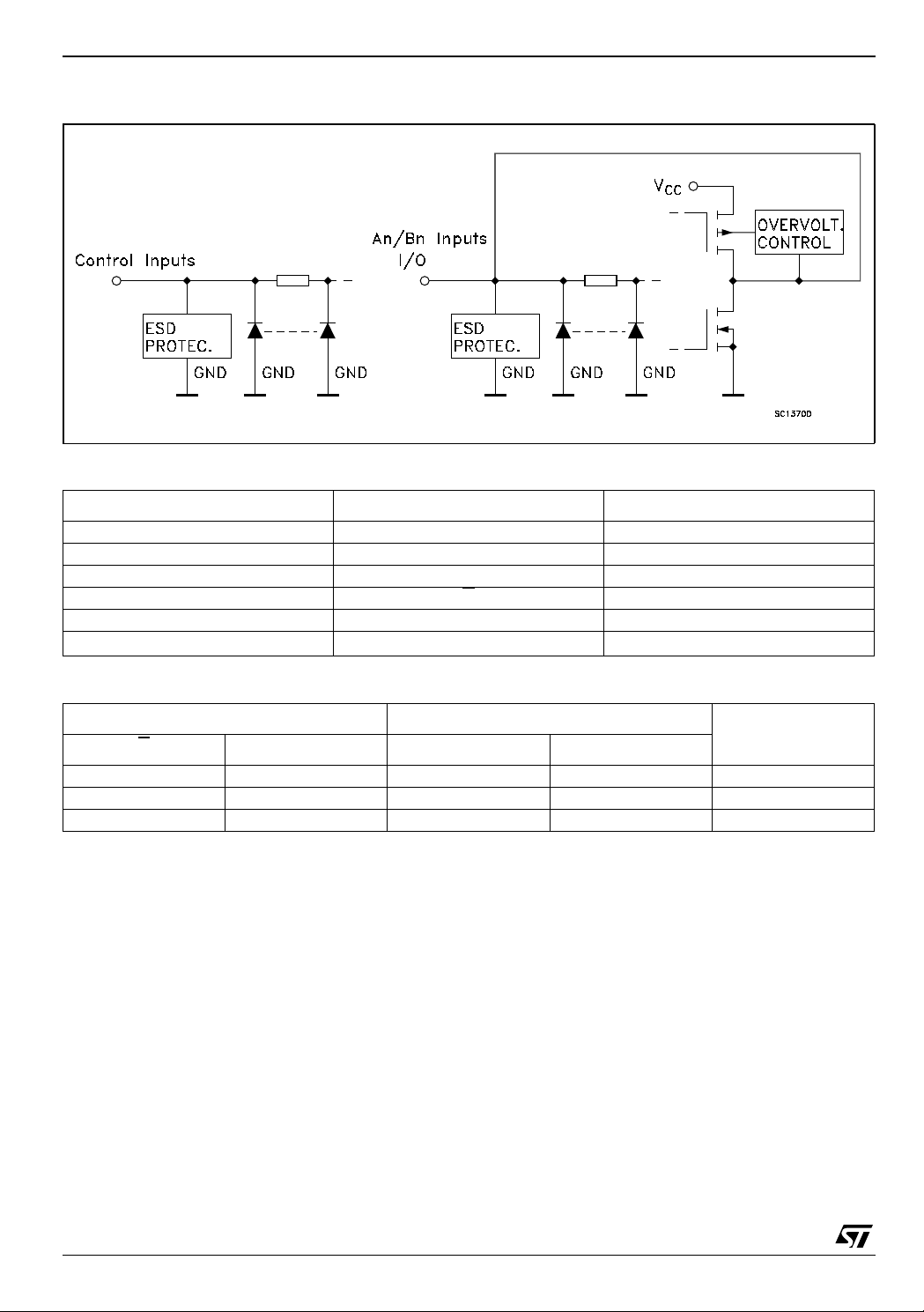
All inputs and outputs are equipped with
protection circuits against static disc harge, giving
them 2KV ESD immunity and transient excess
voltage.
All floating bus terminals during High Z state must
be held HIGH or LOW.
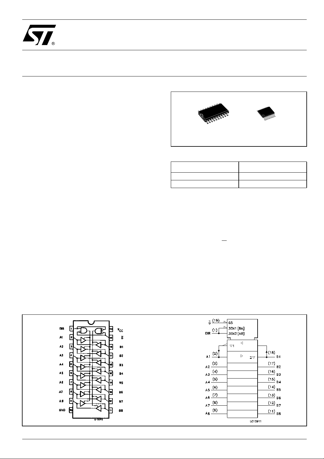
Figure 1: Pin C onnection And I EC Logic Symbol s
Rev. 4
1/13September 2004
74LCX245
Figure 2: Input An d Output Equival e n t Ci rcui t
Table 2: Pin Description
PIN N° SYMBOL NAME AND FUNCTION
1 DIR Directional Control
2, 3, 4, 5, 6, 7, 8, 9 A1 to A8 Data Inputs/Outputs
18, 17, 16, 15, 14, 13, 12, 11 B1 to B8 Data Inputs/Outputs
19 G
10 GND Ground (0V)
20 V
CC
Output Enable Input
Positive Supply Voltage
Table 3: Truth Table
INPUTS FUNCTION
G
L L OUTPUT INPUT A = B
L H INPUT OUTPUT B = A
HXZZZ
X : Don’t Care
Z : High Impedance
DIR A BUS B BUS
OUTPUT
2/13
74LCX245
Table 4: Absolute Maximum Ratings
Symbol Parameter Value Unit
V
V
V
V
I
I
OK
I
I
CC
I
GND
T
T
Absolute Maximum Ratings are those values beyond which damage to the device may occur. Functional operation under these conditions is
not implied
1) I
absolute maximum rating must be observed
O
< GND
2) V
O
Table 5: Recommended Operating Conditions
Supply Voltage
CC
DC Input Voltage
I
DC Output Voltage (OFF State)
O
DC Output Voltage (High or Low State) (note 1) -0.5 to VCC + 0.5
O
DC Input Diode Current
IK
DC Output Diode Current (note 2)
DC Output Current
O
DC Supply Current per Supply Pin
DC Ground Current per Supply Pin
Storage Temperature
stg
Lead Temperature (10 sec)
L
-0.5 to +7.0 V
-0.5 to +7.0 V
-0.5 to +7.0 V
V
- 50 mA
- 50 mA
± 50 mA
± 100 mA
± 100 mA
-65 to +150 °C
300 °C
Symbol Parameter Value Unit
I
I
V
V
V
V
OH
OH
T
Supply Voltage (note 1)
CC
Input Voltage
I
Output Voltage (OFF State)
O
Output Voltage (High or Low State) 0 to V
O
, I
High or Low Level Output Current (VCC = 3.0 to 3.6V)
OL
, I
High or Low Level Output Current (VCC = 2.7V)
OL
Operating Temperature
op
2.0 to 3.6 V
0 to 5.5 V
0 to 5.5 V
CC
± 24 mA
± 12 mA
-55 to 125 °C
dt/dv Input Rise and Fall Time (note 2) 0 to 10 ns/V
1) Truth T abl e guarante ed: 1.5V to 3.6V
from 0.8V to 2V at VCC = 3.0V
2) V
IN
V
3/13
74LCX245
Table 6: DC Specifications
Test Condition Value
Symbol Parameter
V
V
V
V
I
I
OZ
High Level Input
IH
Voltage
Low Level Input
IL
Voltage
High Level Output
OH
Voltage
Low Level Output
OL
Voltage
Input Leakage
I
I
Current
Power Off Leakage
off
Current
High Impedance
Output Leakage
Current
I
CC
∆I
Quiescent Supply
Current
ICC incr. per Input
CC
V
CC
(V)
2.7 to 3.6
2.7 to 3.6
2.7
3.0
2.7 to 3.6
2.7
3.0
2.7 to 3.6
0
2.7 to 3.6
2.7 to 3.6
2.7 to 3.6
-40 to 85 °C -55 to 125 °C
Min. Max. Min. Max.
2.0 2.0 V
0.8 0.8 V
IO=-100 µAVCC-0.2 VCC-0.2
I
=-12 mA
O
=-18 mA
I
O
=-24 mA
I
O
IO=100 µA
I
=12 mA
O
I
=16 mA
O
=24 mA
I
O
= 0 to 5.5V
V
I
or VO = 5.5V
V
I
= VIH or V
V
I
VO = 0 to V
VI = VCC or GND
V
or VO= 3.6 to 5.5V
I
VIH = VCC - 0.6V
IL
CC
2.2 2.2
2.4 2.4
2.2 2.2
0.2 0.2
0.4 0.4
0.4 0.4
0.55 0.55
± 5 ± 5 µA
10 10 µA
± 5 ± 5 µA
10 10
± 10 ± 10
500 500 µA
Unit
V
V
µA
Table 7: Dynamic Switching Characteristics
Test Condition Value
= 25 °C
Symbol Parameter
V
CC
(V)
V
OLP
V
OLV
1) Number of outputs defined as "n". Measured wi t h "n-1" output s switching from HIGH to LO W or LOW to HIGH. The remaining output is
measur ed i n the LOW state.
Dynamic Low Level Quiet
Output (note 1)
3.3
= 50pF
C
L
V
= 0V, VIH = 3.3V
IL
T
A
Min. Typ. Max.
0.8
-0.8
Unit
V
4/13
 Loading...