

Low voltage CMOS Quad 2 channel multiplexer
Features
■ 5V tolerant inputs
■ High speed:
–t
= 6.0ns (Max) at V
PD
■ Power down protection on inputs and outputs
■ Symmetrical output impedance:
–|I
■ PCI bus levels guaranteed at 24mA
■ Balanced propagation delays:
–t
■
Operating voltage range:
–V
■ Pin and function compatible with
| = IOL = 24mA (Min) at VCC = 3V
OH
≅ t
PLH
PHL
(Opr) = 2.0V to 3.6V
CC
74 series 157
■ Latch-up performance exceeds
500mA (JESD 17)
■ ESD performance:
– HBM > 2000V
(MIL STD 883 method 3015); MM > 200V
CC
= 3V
74LCX157
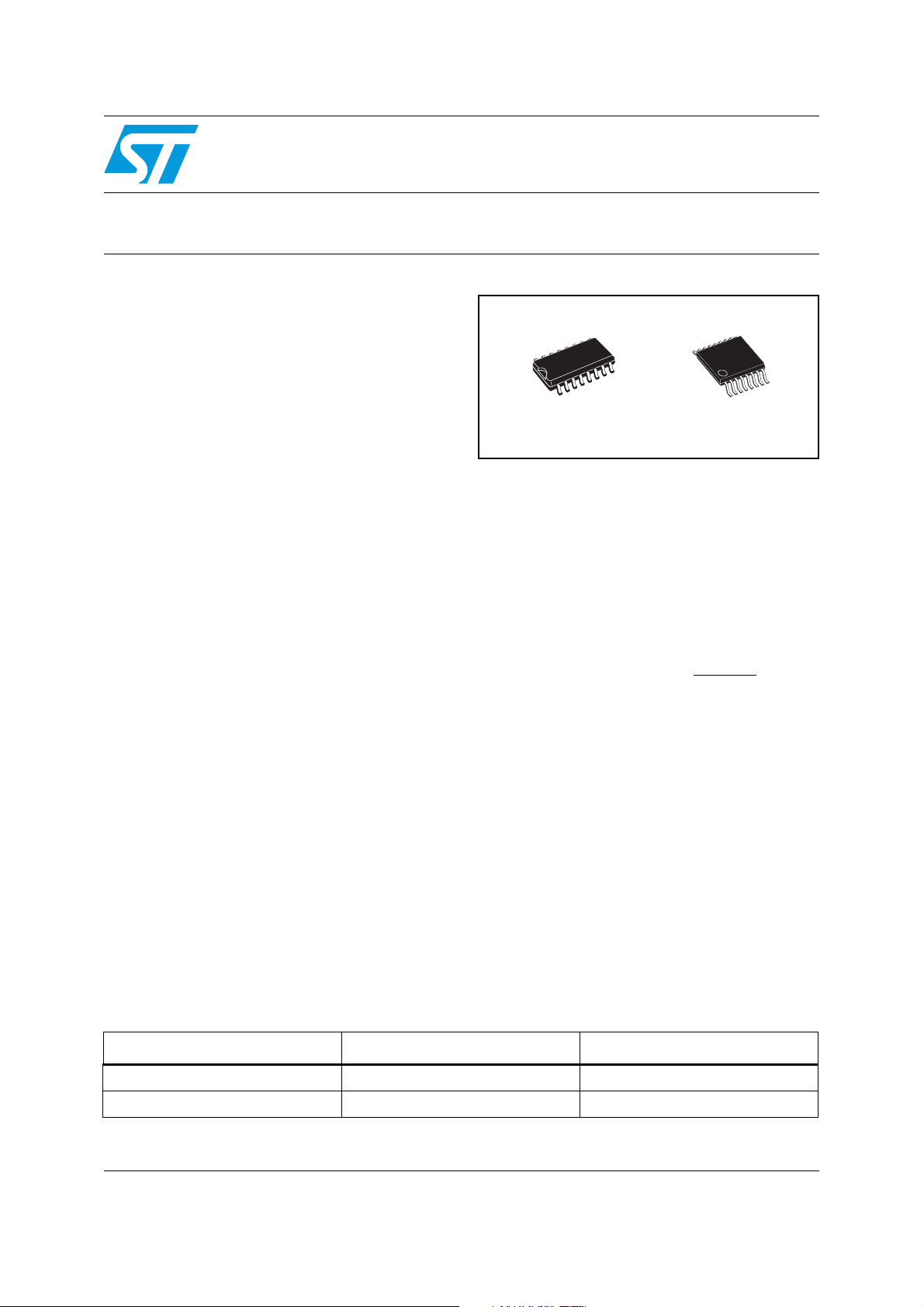
with 5V tolerant inputs
SO-16 TSSOP16
Description
The 74LCX157 is a low voltage CMOS Quad 2
channel multiplexer fabricated with sub-micron
silicon gate and double-layer metal wiring C
technology. It is ideal for low power and high
speed 3.3V applications; it can be interfaced to
5V signal environment for inputs.
It consists of four 2-input digital multiplexer with
common select and strobe inputs. It is a noninverting multiplexer. When the STROBE
held high selection of data is inhibited and all the
outputs become low. The SELECT decoding
determines whether the A or B inputs get routed
to their corresponding Y outputs.
2
MOS
input is
It has same speed performance at 3.3V than 5V
AC/ACT family, combined with a lower power
consumption.
All inputs and outputs are equipped with
protection circuits against static discharge, giving
them 2KV ESD immunity and transient excess
voltage.
Order codes
Part number Package Packaging
74LCX157MTR SO-16 Tape and reel
74LCX157TTR TSSOP16 Tape and reel
February 2007 Rev 6 1/17
www.st.com
17

Contents 74LCX157
Contents
1 Logic symbols and I/O equivalent circuit . . . . . . . . . . . . . . . . . . . . . . . . 3
2 Pin settings . . . . . . . . . . . . . . . . . . . . . . . . . . . . . . . . . . . . . . . . . . . . . . . . 4
2.1 Pin connection . . . . . . . . . . . . . . . . . . . . . . . . . . . . . . . . . . . . . . . . . . . . . . 4
2.2 Pin description . . . . . . . . . . . . . . . . . . . . . . . . . . . . . . . . . . . . . . . . . . . . . . 4
2.3 Truth table . . . . . . . . . . . . . . . . . . . . . . . . . . . . . . . . . . . . . . . . . . . . . . . . . . 5
2.4 Logic diagram . . . . . . . . . . . . . . . . . . . . . . . . . . . . . . . . . . . . . . . . . . . . . . . 5
3 Maximum rating . . . . . . . . . . . . . . . . . . . . . . . . . . . . . . . . . . . . . . . . . . . . . 6
3.1 Recommended operating conditions . . . . . . . . . . . . . . . . . . . . . . . . . . . . . 6
4 Electrical characteristics . . . . . . . . . . . . . . . . . . . . . . . . . . . . . . . . . . . . . 7
5 Test circuit . . . . . . . . . . . . . . . . . . . . . . . . . . . . . . . . . . . . . . . . . . . . . . . . . 9
6 Waveforms . . . . . . . . . . . . . . . . . . . . . . . . . . . . . . . . . . . . . . . . . . . . . . . . 10
7 Package mechanical data . . . . . . . . . . . . . . . . . . . . . . . . . . . . . . . . . . . . 11
8 Revision history . . . . . . . . . . . . . . . . . . . . . . . . . . . . . . . . . . . . . . . . . . . 16
2/17
74LCX157 Logic symbols and I/O equivalent circuit
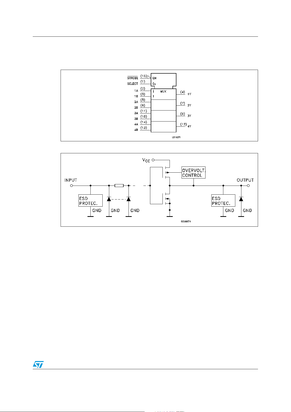
1 Logic symbols and I/O equivalent circuit
Figure 1. IEC logic symbols
Figure 2. Input and output equivalent circuit
3/17
Pin settings 74LCX157
2 Pin settings
2.1 Pin connection
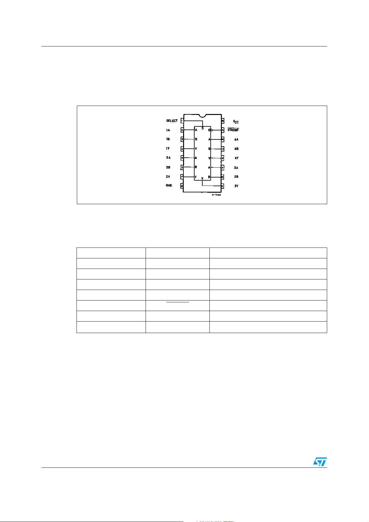
Figure 3. Pin connection (top through view)
2.2 Pin description
Table 1. Pin description
Pin N° Symbol Name and function
1 SELECT Common data select inputs
2, 5, 11, 14 1A to 4A Data inputs from source A
3, 6, 10, 13 1B to 4B Data inputs from source B
4, 7, 9, 12 1Y to 4Y Multiplexer outputs
15 STROBE
8 GND Ground (0V)
16 V
CC
Strobe input
Positive supply voltage
4/17
74LCX157 Pin settings
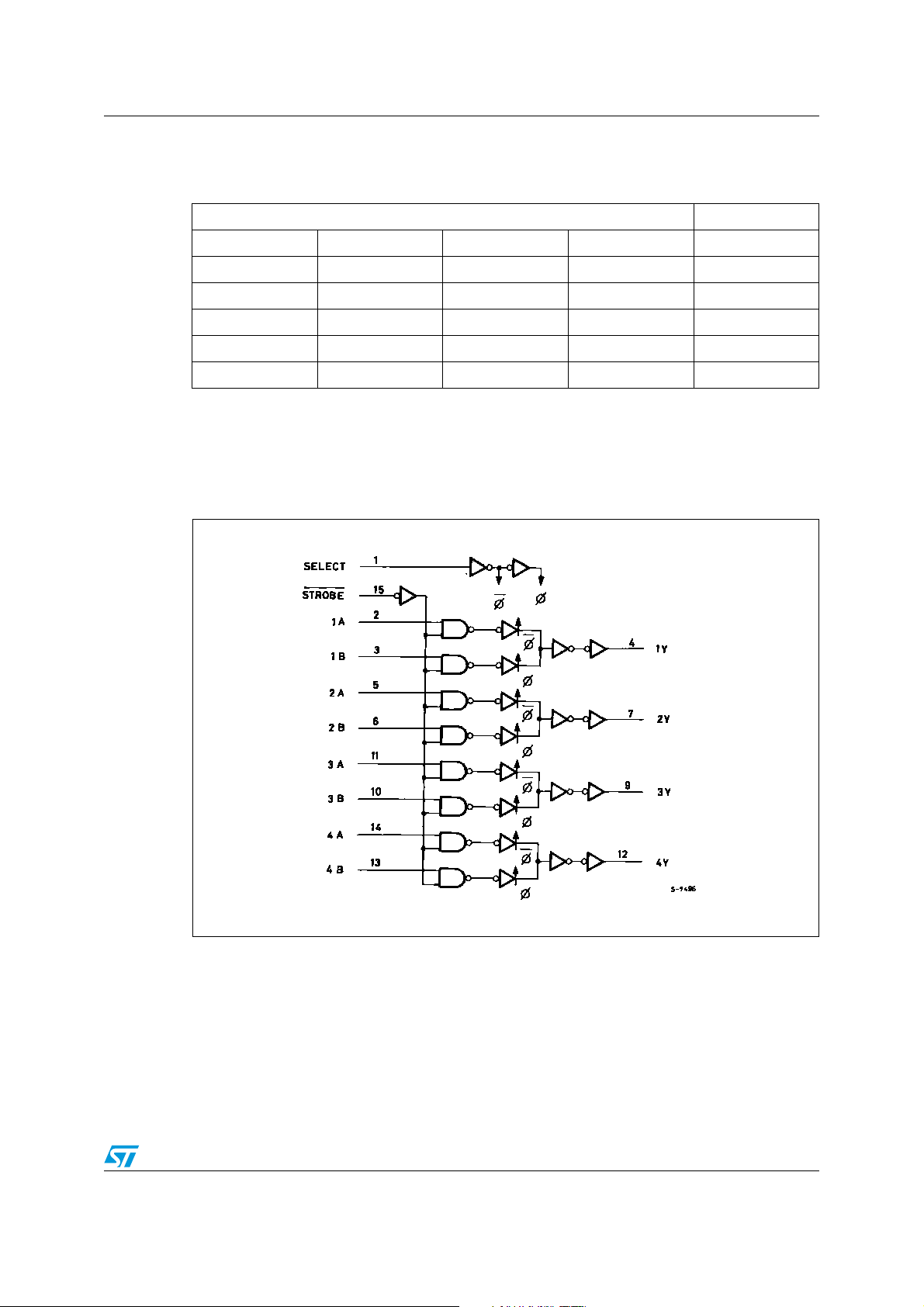
2.3 Truth table
Table 2. Truth table
Inputs Output
STROBE SELECT A B Y
HXXXL
LLLXL
LLHXH
LHXLL
LHXHH
Note: X : Do not care
2.4 Logic diagram
Figure 4. Logic diagram
Note: This logic diagram has not to be used to estimate propagation delays
5/17
Maximum rating 74LCX157
3 Maximum rating
stressing the device above the rating listed in the “absolute maximum ratings” table may
cause permanent damage to the device. these are stress ratings only and operation of the
device at these or any other conditions above those indicated in the operating sections of
this specification is not implied. exposure to absolute maximum rating conditions for
extended periods may affect device reliability. refer also to the STMicroelectronics sure
program and other relevant quality documents.
Table 3. Absolute maximum ratings
Symbol Parameter Value Unit
V
V
V
I
I
I
GND
T
T
1. IO absolute maximum rating must be observed
2. VO < GND
Supply voltage -0.5 to +7.0 V
CC
V
DC input voltage -0.5 to +7.0 V
I
DC output voltage (VCC = 0V)
O
DC output voltage (high or low state)
O
I
DC input diode current -50 mA
IK
DC output diode current
OK
I
DC output current ± 50 mA
O
DC supply current per supply pin ± 100 mA
CC
(2)
(1)
-0.5 to +7.0 V
-0.5 to VCC + 0.5
-50 mA
DC ground current per supply pin ± 100 mA
Storage temperature -65 to +150 °C
stg
Lead temperature (10 sec) 300 °C
L
V
3.1 Recommended operating conditions
Table 4. Recommended operating conditions
Symbol Parameter Value Unit
V
V
V
V
Supply voltage
CC
Input voltage 0 to 5.5 V
I
Output voltage (VCC = 0V)
O
Output voltage (high or low state)
O
IOH, IOLHigh or low level output current (VCC = 3.0 to 3.6V)
I
, IOLHigh or low level output current (VCC = 2.7V)
OH
T
dt/dv
1. Truth table guaranteed: 1.5V to 3.6V
2. VIN from 0.8V to 2V at VCC = 3.0V
Operating temperature -40 to 85 °C
op
Input rise and fall time
6/17
(1)
(2)
2.0 to 3.6 V
0 to 5.5 V
0 to V
CC
± 24 mA
± 12 mA
0 to 10 ns/V
V
 Loading...