

ST 74LCX139 User Manual
查询74LCX139供应商
74LCX139
LOW VOLTAGE CMOS
DUAL 2 TO 4 DECODER/DEMULTIPLEXER
■ 5V TOLERANT INPUTS
■ HIGH SPEED:
t
= 6.2ns (MAX.) at VCC = 3V
PD
■ POWER DOWN PROTECTION ON INPUTS
AND OUTPUTS
■ SYMMETRICAL OUTPUT IMPEDANCE:
|I
| = IOL = 24mA (MIN) at VCC = 3V
OH
■ PCI BUS LEVELS GUARANTEED AT 24 mA
■ BALANCED PROPAGATION DELAYS:
t
≅ t
PLH
PHL
■ OPERATING VOLTAGE RANGE:
V
(OPR) = 2.0V to 3.6V (1.5V Data
CC
Retention)
■ PIN AND FUNCTION COMPATIBLE WITH
74 SERIES 139
■ LA TCH-UP PERFORMANCE EXCEEDS
500mA (JESD 17)
■ ESD PERFORMANCE:
HBM > 2000V (MIL STD 883 method 3015);
MM > 200V
DESCRIPTION
The 74LCX139 is a low voltage CMOS DU AL 2
TO 4 LINE DECODER/DEMULTIPLEXER
fabricated with sub-micron silicon gate and
double-layer metal wiring C
2
MOS technology.
It is ideal for low power and high speed 3.3V
applications; it can be interfaced to 5V signal
environment for inputs.
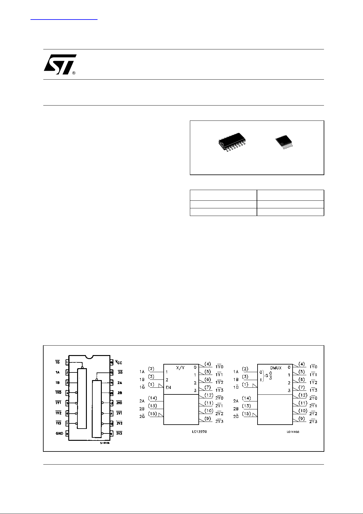
TSSOPSOP
Table 1: Order Codes
PACKAGE T & R
SOP 74LCX139MTR
TSSOP 74LCX139TTR
The active low enable input can be used for gating
or as a data input for demultiplexing applications.
While the enable input is held high, all four outputs
are high independently of the other inputs.
It has same speed performance at 3.3V than 5V
AC/ACT family, combined with a lower power
consumption.
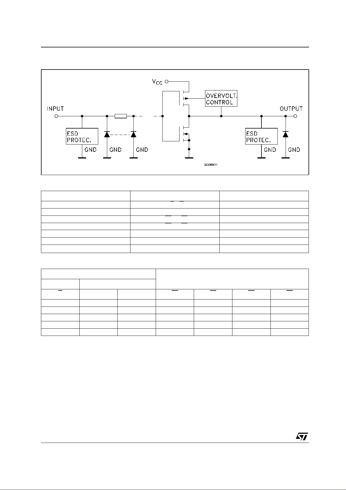
All inputs and outputs are equipped with
protection circuits against static disc harge, giving
them 2KV ESD immunity and transient excess
voltage.
Figure 1: Pin C onnection And I EC Logic Symbol s
Rev. 3
1/12September 2004
74LCX139
Figure 2: Input An d Output Equival e n t Ci rcui t
Table 2: Pin Description
PIN N° SYMBOL NAME AND FUNCTION
1, 15 1G
2, 3 1A, 1B Address Inputs
4, 5, 6, 7 1Y0
12, 11, 10, 9 2Y0
14, 13 2A, 2B Address Inputs
8 GND Ground (0V)
16 V
, 2G Enable Inputs
to 1Y3 Outputs
to 2Y3 Outputs
CC
Positive Supply Voltage
Table 3: Truth Table
INPUTS
ENABLE SELECT
G
HXXHHHH
LLLLHHH
LLHHLHH
LHLHHLH
LHHHHHL
X : Don’t Care
BAY0Y1 Y2 Y3
OUTPUTS
2/12
74LCX139
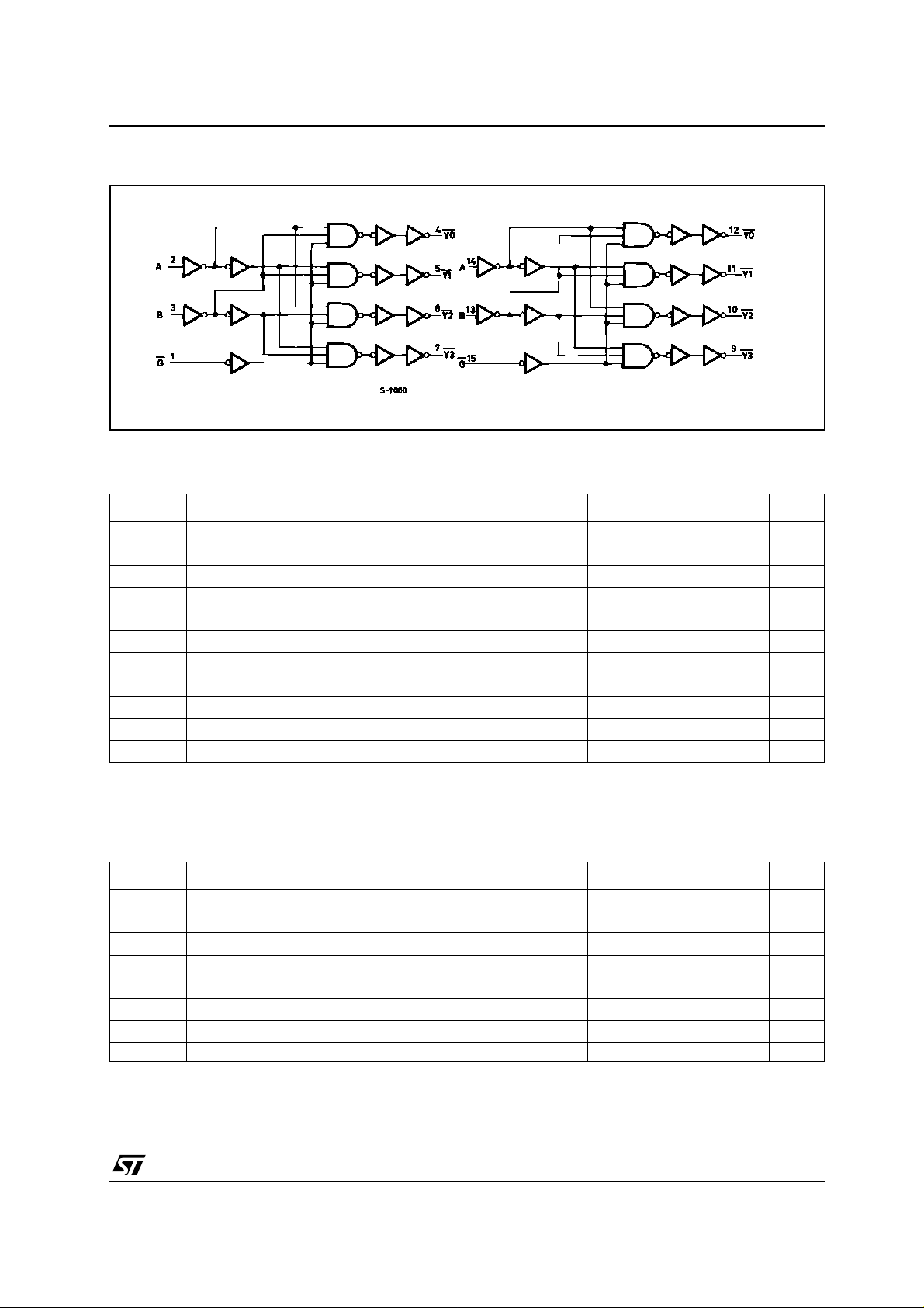
Figure 3: Logic Diagram
This logi c di agram has not be used to estim ate propaga tion delays
Table 4: Absolute Maximum Ratings
Symbol Parameter Value Unit
V
V
V
V
I
I
OK
I
I
CC
I
GND
T
T
Absolute Maximum Ratings are those values beyond which damage to the device may occur. Functional operation under these conditions is
not implied
1) I
absolute maximum rating must be observed
O
< GND
2) V
O
Table 5: Recommended Operating Conditions
Supply Voltage
CC
DC Input Voltage
I
DC Output Voltage (VCC = 0V)
O
DC Output Voltage (High or Low State) (note 1) -0.5 to VCC + 0.5
O
DC Input Diode Current
IK
DC Output Diode Current (note 2)
DC Output Current
O
DC Supply Current per Supply Pin
DC Ground Current per Supply Pin
Storage Temperature
stg
Lead Temperature (10 sec)
L
-0.5 to +7.0 V
-0.5 to +7.0 V
-0.5 to +7.0 V
V
- 50 mA
- 50 mA
± 50 mA
± 100 mA
± 100 mA
-65 to +150 °C
300 °C
Symbol Parameter Value Unit
I
I
V
V
V
V
OH
OH
T
Supply Voltage (note 1)
CC
Input Voltage
I
Output Voltage (VCC = 0V)
O
Output Voltage (High or Low State) 0 to V
O
, I
High or Low Level Output Current (VCC = 3.0 to 3.6V)
OL
, I
High or Low Level Output Current (VCC = 2.7V)
OL
Operating Temperature
op
2.0 to 3.6 V
0 to 5.5 V
0 to 5.5 V
CC
± 24 mA
± 12 mA
-55 to 125 °C
dt/dv Input Rise and Fall Time (note 2) 0 to 10 ns/V
1) Truth T abl e guarante ed: 1.5V to 3.6V
2) VIN from 0.8V to 2V at VCC = 3.0V
V
3/12
74LCX139
Table 6: DC Specifications
Test Condition Value
Symbol Parameter
V
CC
(V)
V
V
V
V
I
I
CC
∆I
High Level Input
IH
Voltage
Low Level Input
IL
Voltage
High Level Output
OH
Voltage
Low Level Output
OL
Voltage
Input Leakage
I
I
Current
Power Off Leakage
off
Current
Quiescent Supply
Current
ICC incr. per Input
CC
2.7 to 3.6
2.7 to 3.6
2.7
3.0
2.7 to 3.6
2.7
3.0
2.7 to 3.6
0
2.7 to 3.6
2.7 to 3.6
IO=-100 µAVCC-0.2 VCC-0.2
I
=-12 mA
O
=-18 mA
I
O
=-24 mA
I
O
IO=100 µA
I
=12 mA
O
I
=16 mA
O
=24 mA
I
O
= 0 to 5.5V
V
I
or VO = 5.5V
V
I
VI = VCC or GND
or VO= 3.6 to 5.5V
V
I
VIH = VCC - 0.6V
Table 4: DYNAMIC SWITCHING CHARACTERISTICS
-40 to 85 °C -55 to 125 °C
Min. Max. Min. Max.
2.0 2.0 V
0.8 0.8 V
2.2 2.2
2.4 2.4
2.2 2.2
0.2 0.2
0.4 0.4
0.4 0.4
0.55 0.55
± 5 ± 5 µA
10 10 µA
10 10
± 10 ± 10
500 500 µA
Unit
V
V
µA
Test Condition Value
= 25 °C
Symbol Parameter
V
CC
(V)
V
OLP
V
OLV
1) Number of outputs defined as "n". Measured wi t h "n-1" output s switching from HIGH to LO W or LOW to HIGH. The remaining output is
measur ed i n the LOW state.
Dynamic Low Level Quiet
Output (note 1)
3.3
= 50pF
C
L
V
= 0V, VIH = 3.3V
IL
T
A
Min. Typ. Max.
0.8
-0.8
Unit
V
Table 7: AC Electrical Characteristics
Test Condition Value
Symbol Parameter
t
PLH tPHL
t
PLH tPHL
t
OSLH
t
OSHL
1) Skew is defined as the absolute value of the difference between the actual propagation delay for any two outputs of the same device switching in the sa me directio n, either HIGH or LOW (t
2) Param eter guaran teed by design
Propagation Delay
Time A, B to Y
Propagation Delay
to Y
Time G
Output To Output
Skew Time (note1,
2)
V
CC
(V)
2.7
3.0 to 3.6 1.0 6.2 1.0 6.2
2.7
3.0 to 3.6 1.0 5.3 1.0 5.3
C
R
L
(pF)
(Ω)
50 500 2.5
50 500 2.5
= t
t
L
s
(ns)
3.0 to 3.6 50 500 2.5 1.0 1.0 ns
OSLH
= | t
PLHm
- t
PLHn
|, t
OSHL
= | t
-40 to 85 °C -55 to 125 °C
r
Min. Max. Min. Max.
7.3 7.3
5.8 5.8
- t
PHLn
|)
PHLm
Unit
ns
ns
4/12
 Loading...