74LCX138MTR
74LCX138
LOW VOLTAGE CMOS 3 TO 8 LINE DECODER (INV.) WITH 5V TOLERANT INPUTS
■5V TOLERANT INPUTS
■HIGH SPEED:
tPD = 6.7ns (MAX.) at VCC = 3V
■POWER DOWN PROTECTION ON INPUTS AND OUTPUTS
■SYMMETRICAL OUTPUT IMPEDANCE: |IOH| = IOL = 24mA (MIN) at VCC = 3V
■PCI BUS LEVELS GUARANTEED AT 24 mA
■BALANCED PROPAGATION DELAYS: tPLH tPHL
■OPERATING VOLTAGE RANGE:
VCC(OPR) = 2.0V to 3.6V (1.5V Data Retention)
■PIN AND FUNCTION COMPATIBLE WITH 74 SERIES 138
■LATCH-UP PERFORMANCE EXCEEDS 500mA (JESD 17)
■ESD PERFORMANCE:
HBM > 2000V (MIL STD 883 method 3015); MM > 200V
DESCRIPTION
The 74LCX138 is a low voltage CMOS 3 TO 8 LINE DECODER (INVERTING) fabricated with sub-micron silicon gate and double-layer metal wiring C2MOS technology. It is ideal for low power and high speed 3.3V applications; it can be interfaced to 5V signal environment for inputs.
If the device is enabled, 3 binary select inputs (A, B and C) determine which one of the outputs will
SOP TSSOP
Table 1: Order Codes
PACKAGE |
T & R |
|
|
SOP |
74LCX138MTR |
|
|
TSSOP |
74LCX138TTR |
|
|
go low. If enable input G1 is held low or either G2A or G2B is held high, the decoding function is inhibited and all the 8 outputs go to high.
Three enable inputs are provided to ease cascade connection and application of address decoders for memory systems.
It has same speed performance at 3.3V than 5V AC/ACT family, combined with a lower power consumption.
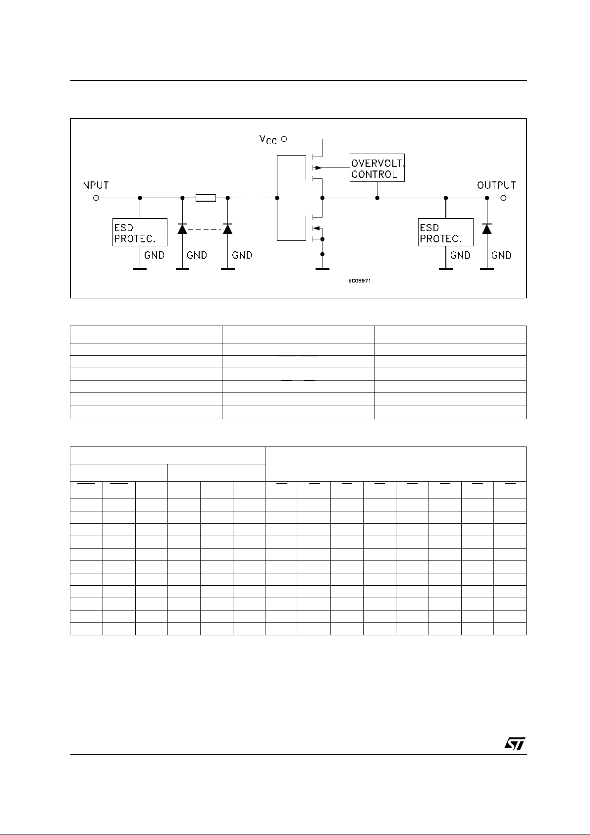
All inputs and outputs are equipped with protection circuits against static discharge, giving them 2KV ESD immunity and transient excess voltage.
Figure 1: Pin Connection And IEC Logic Symbols
September 2004 |
Rev. 4 |
1/12 |
|
|
|
74LCX138
Figure 2: Input And Output Equivalent Circuit
Table 2: Pin Description
|
|
|
|
|
PIN N° |
|
|
|
|
|
|
|
SYMBOL |
|
|
|
|
|
NAME AND FUNCTION |
|
|
||||||||||||||||||||||
|
|
|
|
|
|
|
|
|
|
|
|
|
|
|
|
|
|
|
|
|
|
|
|
|
|
|
|
|
|
|
|
||||||||||||
|
|
|
|
|
1, 2, 3 |
|
|
|
|
|
|
|
|
A, B, C |
|
|
|
Address Inputs |
|
|
|
|
|
|
|
|
|||||||||||||||||
|
|
|
|
|
|
|
|
|
|
|
|
|
|
|
|
|
|
|
|
|
|
|
|
|
|
|
|
|
|
|
|
|
|
|
|
|
|
|
|
|
|||
|
|
|
|
|
4, 5 |
|
|
|
|
|
|
|
G2A, |
|
|
G2B |
|
|
|
|
|
|
Enable Inputs |
|
|
|
|
|
|
|
|
||||||||||||
|
|
|
|
|
|
|
|
|
|
|
|
|
|
|
|
|
|
|
|
|
|
|
|
|
|
|
|
|
|
|
|
|
|
||||||||||
|
|
|
|
|
6 |
|
|
|
|
|
|
|
|
|
|
G1 |
|
|
|
Enable Input |
|
|
|
|
|
|
|
|
|||||||||||||||
|
|
|
|
|
|
|
|
|
|
|
|
|
|
|
|
|
|
|
|
|
|
|
|
|
|
|
|
|
|
|
|
|
|
|
|
||||||||
|
|
15, 14, 13, 12, 11, 10, 9, 7 |
|
|
|
|
|
|
|
Y0 |
to |
Y7 |
|
|
|
|
|
|
Outputs |
|
|
|
|
|
|
|
|
||||||||||||||||
|
|
|
|
|
|
|
|
|
|
|
|
|
|
|
|
|
|
|
|
|
|
|
|
|
|
|
|
|
|
|
|
|
|||||||||||
|
|
|
|
|
8 |
|
|
|
|
|
|
|
|
|
GND |
|
|
|
Ground (0V) |
|
|
|
|
|
|
|
|
||||||||||||||||
|
|
|
|
|
|
|
|
|
|
|
|
|
|
|
|
|
|
|
|
|
|
|
|
|
|
|
|
|
|
|
|||||||||||||
|
|
|
|
|
16 |
|
|
|
|
|
|
|
|
|
VCC |
|
|
|
Positive Supply Voltage |
|
|
|
|
|
|||||||||||||||||||
Table 3: Truth Table |
|
|
|
|
|
|
|
|
|
|
|
|
|
|
|
|
|
|
|
|
|
|
|
|
|
|
|
|
|
|
|
|
|
|
|
|
|
||||||
|
|
|
|
|
|
|
|
|
|
|
|
|
|
|
|
|
|
|
|
|
|
|
|
|
|
|
|
|
|
|
|
|
|
|
|
|
|
|
|
|
|
|
|
|
|
|
|
|
|
INPUTS |
|
|
|
|
|
|
|
|
|
|
|
|
|
|
|
|
|
|
|
|
|
|
OUTPUTS |
|
|
|
|
|
|
|
|
||||||
|
|
|
|
|
|
|
|
|
|
|
|
|
|
|
|
|
|
|
|
|
|
|
|
|
|
|
|
|
|
|
|
|
|
|
|
|
|
||||||
|
|
ENABLE |
|
SELECT |
|
|
|
|
|
|
|
|
|
|
|
|
|
|
|
|
|
|
|
|
|
|
|
|
|
|
|
||||||||||||
|
|
|
|
|
|
|
|
|
|
|
|
|
|
|
|
|
|
|
|
|
|
|
|
|
|
|
|
|
|
|
|
|
|
|
|
||||||||
|
|
|
|
|
|
|
|
|
|
|
|
|
|
|
|
|
|
|
|
|
|
|
|
|
|
|
|
|
|
|
|
|
|
|
|
|
|
|
|
||||
|
G2B |
|
|
G2A |
|
G1 |
C |
B |
|
A |
|
Y0 |
|
|
|
|
|
|
Y1 |
|
Y2 |
|
|
Y3 |
|
|
Y4 |
|
Y5 |
|
Y6 |
|
Y7 |
|
|||||||||
|
|
|
|
|
|
|
|
|
|
|
|
|
|
|
|
|
|
|
|
|
|
|
|
|
|
|
|
|
|
|
|
|
|
|
|
||||||||
|
X |
|
|
X |
|
L |
X |
X |
|
X |
|
|
H |
|
|
|
|
|
|
H |
|
H |
|
|
H |
|
|
H |
|
H |
|
H |
|
H |
|
||||||||
|
|
|
|
|
|
|
|
|
|
|
|
|
|
|
|
|
|
|
|
|
|
|
|
|
|
|
|
|
|
|
|
|
|
|
|
||||||||
|
X |
|
|
H |
|
X |
X |
X |
|
X |
|
|
H |
|
|
|
|
|
|
H |
|
H |
|
|
H |
|
|
H |
|
H |
|
H |
|
H |
|
||||||||
|
|
|
|
|
|
|
|
|
|
|
|
|
|
|
|
|
|
|
|
|
|
|
|
|
|
|
|
|
|
|
|
|
|
|
|
||||||||
|
H |
|
|
X |
|
X |
X |
X |
|
X |
|
|
H |
|
|
|
|
|
|
H |
|
H |
|
|
H |
|
|
H |
|
H |
|
H |
|
H |
|
||||||||
|
|
|
|
|
|
|
|
|
|
|
|
|
|
|
|
|
|
|
|
|
|
|
|
|
|
|
|
|
|
|
|
|
|
|
|
||||||||
|
L |
|
|
L |
|
H |
L |
L |
|
L |
|
|
L |
|
|
|
|
|
|
H |
|
H |
|
|
H |
|
|
H |
|
H |
|
H |
|
H |
|
||||||||
|
|
|
|
|
|
|
|
|
|
|
|
|
|
|
|
|
|
|
|
|
|
|
|
|
|
|
|
|
|
|
|
|
|
|
|
||||||||
|
L |
|
|
L |
|
H |
L |
L |
|
H |
|
|
H |
|
|
|
|
|
|
L |
|
H |
|
|
H |
|
|
H |
|
H |
|
H |
|
H |
|
||||||||
|
|
|
|
|
|
|
|
|
|
|
|
|
|
|
|
|
|
|
|
|
|
|
|
|
|
|
|
|
|
|
|
|
|
|
|
||||||||
|
L |
|
|
L |
|
H |
L |
H |
|
L |
|
|
H |
|
|
|
|
|
|
H |
|
L |
|
|
H |
|
|
H |
|
H |
|
H |
|
H |
|
||||||||
|
|
|
|
|
|
|
|
|
|
|
|
|
|
|
|
|
|
|
|
|
|
|
|
|
|
|
|
|
|
|
|
|
|
|
|
||||||||
|
L |
|
|
L |
|
H |
L |
H |
|
H |
|
|
H |
|
|
|
|
|
|
H |
|
H |
|
|
L |
|
|
H |
|
H |
|
H |
|
H |
|
||||||||
|
|
|
|
|
|
|
|
|
|
|
|
|
|
|
|
|
|
|
|
|
|
|
|
|
|
|
|
|
|
|
|
|
|
|
|
||||||||
|
L |
|
|
L |
|
H |
H |
L |
|
L |
|
|
H |
|
|
|
|
|
|
H |
|
H |
|
|
H |
|
|
L |
|
H |
|
H |
|
H |
|
||||||||
|
|
|
|
|
|
|
|
|
|
|
|
|
|
|
|
|
|
|
|
|
|
|
|
|
|
|
|
|
|
|
|
|
|
|
|
||||||||
|
L |
|
|
L |
|
H |
H |
L |
|
H |
|
|
H |
|
|
|
|
|
|
H |
|
H |
|
|
H |
|
|
H |
|
L |
|
H |
|
H |
|
||||||||
|
|
|
|
|
|
|
|
|
|
|
|
|
|
|
|
|
|
|
|
|
|
|
|
|
|
|
|
|
|
|
|
|
|
|
|
||||||||
|
L |
|
|
L |
|
H |
H |
H |
|
L |
|
|
H |
|
|
|
|
|
|
H |
|
H |
|
|
H |
|
|
H |
|
H |
|
L |
|
H |
|
||||||||
|
|
|
|
|
|
|
|
|
|
|
|
|
|
|
|
|
|
|
|
|
|
|
|
|
|
|
|
|
|
|
|
|
|
|
|
||||||||
|
L |
|
|
L |
|
H |
H |
H |
|
H |
|
|
H |
|
|
|
|
|
|
H |
|
H |
|
|
H |
|
|
H |
|
H |
|
H |
|
L |
|
X : Don’t Care
2/12
74LCX138
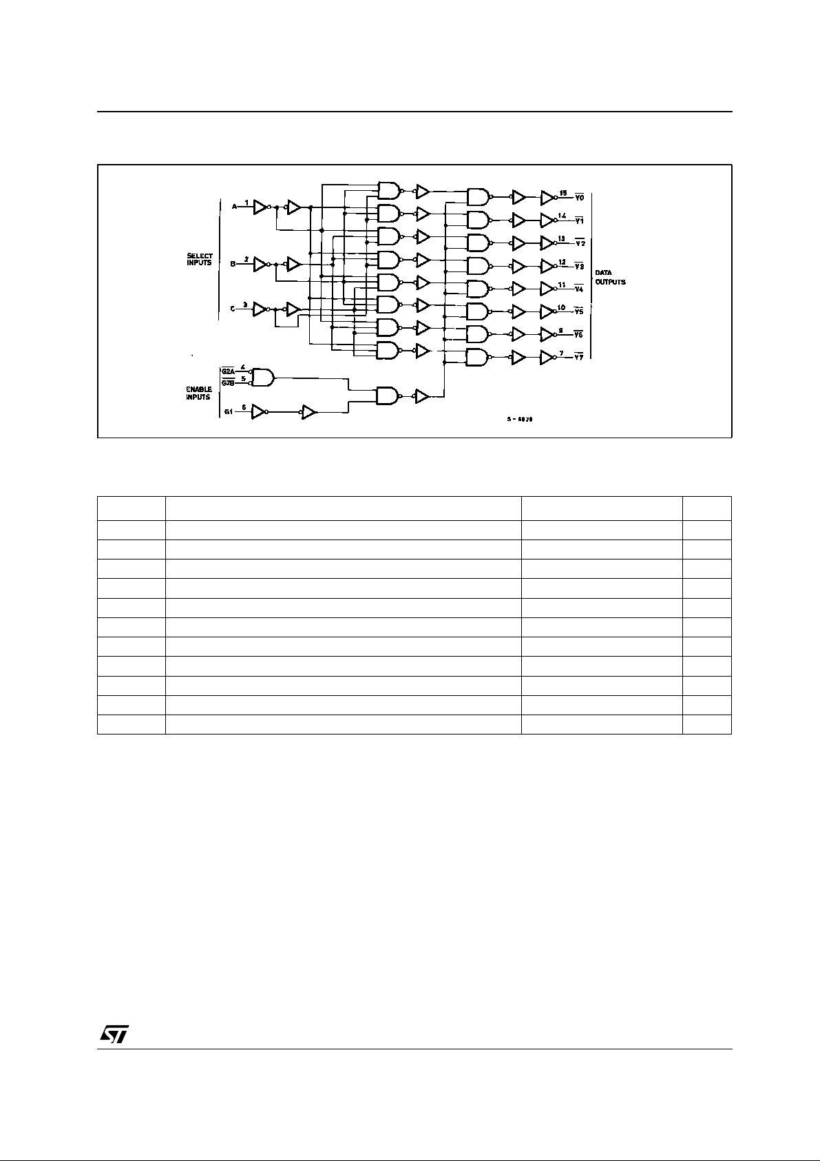
Figure 3: Logic Diagram
This logic diagram has not be used to estimate propagation delays
Table 4: Absolute Maximum Ratings
Symbol |
Parameter |
Value |
Unit |
|
|
|
|
|
|
VCC |
Supply Voltage |
-0.5 to +7.0 |
V |
|
VI |
DC Input Voltage |
-0.5 to +7.0 |
V |
|
VO |
DC Output Voltage (VCC = 0V) |
-0.5 to +7.0 |
V |
|
VO |
DC Output Voltage (High or Low State) (note 1) |
-0.5 to VCC + 0.5 |
V |
|
IIK |
DC Input Diode Current |
- 50 |
mA |
|
IOK |
DC Output Diode Current (note 2) |
- 50 |
mA |
|
IO |
DC Output Current |
± |
50 |
mA |
ICC |
DC Supply Current per Supply Pin |
± |
100 |
mA |
IGND |
DC Ground Current per Supply Pin |
± |
100 |
mA |
Tstg |
Storage Temperature |
-65 to +150 |
°C |
|
TL |
Lead Temperature (10 sec) |
300 |
°C |
Absolute Maximum Ratings are those values beyond which damage to the device may occur. Functional operation under these conditions is not implied
1)IO absolute maximum rating must be observed
2)VO < GND
3/12
74LCX138
Table 5: Recommended Operating Conditions
Symbol |
Parameter |
Value |
Unit |
|
|
|
|
|
|
VCC |
Supply Voltage (note 1) |
2.0 to 3.6 |
V |
|
VI |
Input Voltage |
0 to 5.5 |
V |
|
VO |
Output Voltage (VCC = 0V) |
0 to 5.5 |
V |
|
VO |
Output Voltage (High or Low State) |
0 to VCC |
V |
|
IOH, IOL |
High or Low Level Output Current (VCC = 3.0 to 3.6V) |
± |
24 |
mA |
IOH, IOL |
High or Low Level Output Current (VCC = 2.7V) |
± |
12 |
mA |
Top |
Operating Temperature |
-55 to 125 |
°C |
|
dt/dv |
Input Rise and Fall Time (note 2) |
0 to 10 |
ns/V |
|
|
|
|
|
|
1)Truth Table guaranteed: 1.5V to 3.6V
2)VIN from 0.8V to 2V at VCC = 3.0V
Table 6: DC Specifications
|
|
Test Condition |
|
|
|
Value |
|
|
||||||||
Symbol |
Parameter |
|
|
|
|
|
|
|
|
|
|
|
|
Unit |
||
VCC |
|
|
|
-40 to 85 °C |
|
-55 to 125 °C |
||||||||||
|
|
|
|
|
|
|
|
|
|
|
|
|
|
|
||
|
|
(V) |
|
|
|
Min. |
|
Max. |
|
Min. |
|
|
Max. |
|
||
|
|
|
|
|
|
|
|
|
|
|
|
|||||
|
|
|
|
|
|
|
|
|
|
|
|
|
|
|
|
|
VIH |
High Level Input |
|
|
|
|
|
2.0 |
|
|
|
2.0 |
|
|
|
V |
|
|
Voltage |
2.7 to 3.6 |
|
|
|
|
|
|
|
|
|
|
|
|
|
|
VIL |
Low Level Input |
|
|
|
|
|
0.8 |
|
|
|
|
0.8 |
V |
|||
|
|
|
|
|
|
|
|
|
|
|
||||||
|
Voltage |
|
|
|
|
|
|
|
|
|
|
|
|
|
|
|
VOH |
High Level Output |
2.7 to 3.6 |
IO=-100 A |
VCC-0.2 |
|
|
|
VCC-0.2 |
|
|
|
|
||||
|
Voltage |
|
|
|
|
|
|
|
|
|
|
|
|
|
|
|
|
2.7 |
|
IO=-12 mA |
2.2 |
|
|
|
2.2 |
|
|
|
V |
||||
|
|
|
|
|
|
|
|
|
||||||||
|
|
3.0 |
|
IO=-18 mA |
2.4 |
|
|
|
2.4 |
|
|
|
||||
|
|
|
|
|
|
|
|
|
|
|||||||
|
|
|
IO=-24 mA |
2.2 |
|
|
|
2.2 |
|
|
|
|
||||
|
|
|
|
|
|
|
|
|
|
|
||||||
VOL |
Low Level Output |
2.7 to 3.6 |
IO=100 A |
|
|
0.2 |
|
|
|
|
0.2 |
|
||||
|
Voltage |
|
|
|
|
|
|
|
|
|
|
|
|
|
|
|
|
2.7 |
|
IO=12 mA |
|
|
0.4 |
|
|
|
|
0.4 |
V |
||||
|
|
|
|
|
|
|
|
|
||||||||
|
|
3.0 |
|
IO=16 mA |
|
|
0.4 |
|
|
|
|
0.4 |
||||
|
|
|
|
|
|
|
|
|
|
|||||||
|
|
|
IO=24 mA |
|
|
0.55 |
|
|
|
|
0.55 |
|
||||
|
|
|
|
|
|
|
|
|
|
|
||||||
II |
Input Leakage |
2.7 to 3.6 |
VI = 0 to 5.5V |
|
|
± 5 |
|
|
|
|
± 5 |
A |
||||
|
Current |
|
|
|
|
|
|
|||||||||
|
|
|
|
|
|
|
|
|
|
|
|
|
|
|
|
|
Ioff |
Power Off Leakage |
0 |
|
VI or VO = 5.5V |
|
|
10 |
|
|
|
|
10 |
A |
|||
|
Current |
|
|
|
|
|
|
|
||||||||
|
|
|
|
|
|
|
|
|
|
|
|
|
|
|
|
|
ICC |
Quiescent Supply |
2.7 to 3.6 |
VI = VCC or GND |
|
|
10 |
|
|
|
|
10 |
A |
||||
|
Current |
|
|
|
|
|
|
|
|
|
|
|
|
|||
|
VI or VO= 3.6 to 5.5V |
|
|
± 10 |
|
|
|
|
± 10 |
|||||||
|
|
|
|
|
|
|
|
|
|
|
||||||
∆ ICC |
ICC incr. per Input |
2.7 to 3.6 |
VIH = VCC - 0.6V |
|
|
500 |
|
|
|
|
500 |
A |
||||
Table 7: Dynamic Switching Characteristics |
|
|
|
|
|
|
|
|
|
|
|
|
||||
|
|
|
|
|
|
|
|
|
|
|
|
|
|
|||
|
|
|
|
|
Test Condition |
|
|
|
Value |
|
|
|||||
|
|
|
|
|
|
|
|
|
|
|
|
|
|
|
|
|
Symbol |
Parameter |
|
|
VCC |
|
|
|
|
|
|
TA = 25 °C |
|
Unit |
|||
|
|
|
|
|
|
|
|
|
|
|
|
|
|
|
|
|
|
|
|
|
(V) |
|
|
|
|
|
Min. |
|
Typ. |
|
Max. |
|
|
|
|
|
|
|
|
|
|
|
|
|
|
|
||||
|
|
|
|
|
|
|
|
|
|
|
|
|
|
|||
VOLP |
Dynamic Low Level Quiet |
|
3.3 |
|
CL = 50pF |
|
|
|
0.8 |
|
|
|
V |
|||
|
Output (note 1) |
|
|
|
VIL = 0V, VIH = 3.3V |
|
|
|
|
|
|
|
||||
VOLV |
|
|
|
|
|
|
-0.8 |
|
|
|
||||||
|
|
|
|
|
|
|
|
|
|
|
|
1) Number of outputs defined as "n". Measured with "n-1" outputs switching from HIGH to LOW or LOW to HIGH. The remaining output is measured in the LOW state.
4/12