

ST 74LCX00 User Manual
查询74LCX00MTR供应商
LOW VOLTAGE CMOS QUAD 2-INPUT NAND GATE
74LCX00
WITH 5V TOLERANT INPUTS
■ 5V TOLERANT INPUTS
■ HIGH SPEED :
t
= 4.3ns (MAX.) at VCC = 3V
PD
■ POWER DOWN PROTECTION ON INPUT S
AND OUTPUTS
■ SYMMETRICAL OUTPUT IMPEDANCE:
|I
| = IOL = 24mA (MIN) at VCC = 3V
OH
■ PCI BUS LEVELS GUARANT EED AT 2 4 mA
■ BALANCED PROPAGATION DELAYS:
t
≅ t
PLH
■ OPERATING VOLTAGE RANGE:
V
CC
PHL
(OPR) = 2.0V to 3.6V (1.5V Data
Retention)
■ PIN AND FUNCTION COMPATIBLE WITH
74 SERIES 00
■ LATCH-UP PERFORMANCE EXCEEDS
500mA (JESD 17)
■ ESD PERFORMANCE:
HBM > 2000V (MIL STD 883 method 3015);
MM > 200V
DESCRIPTION
The 74LCX00 is a low voltage CMOS QUAD
2-INPUT NAND GATE fabricated with sub-micron
silicon gate and double-layer metal wiring C
2
MOS
TSSOPSOP
ORDER CODES
PACKAGE TUBE T & R
SOP 74LCX00M 74LCX00MTR
TSSOP 74LCX00TTR
technology. It is ideal for low power and high
speed 3.3V applications; it can be interfaced to 5V
signal environment for inputs.
It has same speed performance at 3. 3V than 5V
AC/ACT family, combined with a lower power
consumption.
All inputs and outputs are equipped with
protection circuits against stat ic discharge, giving
them 2KV ESD immunity and transient excess
voltage.
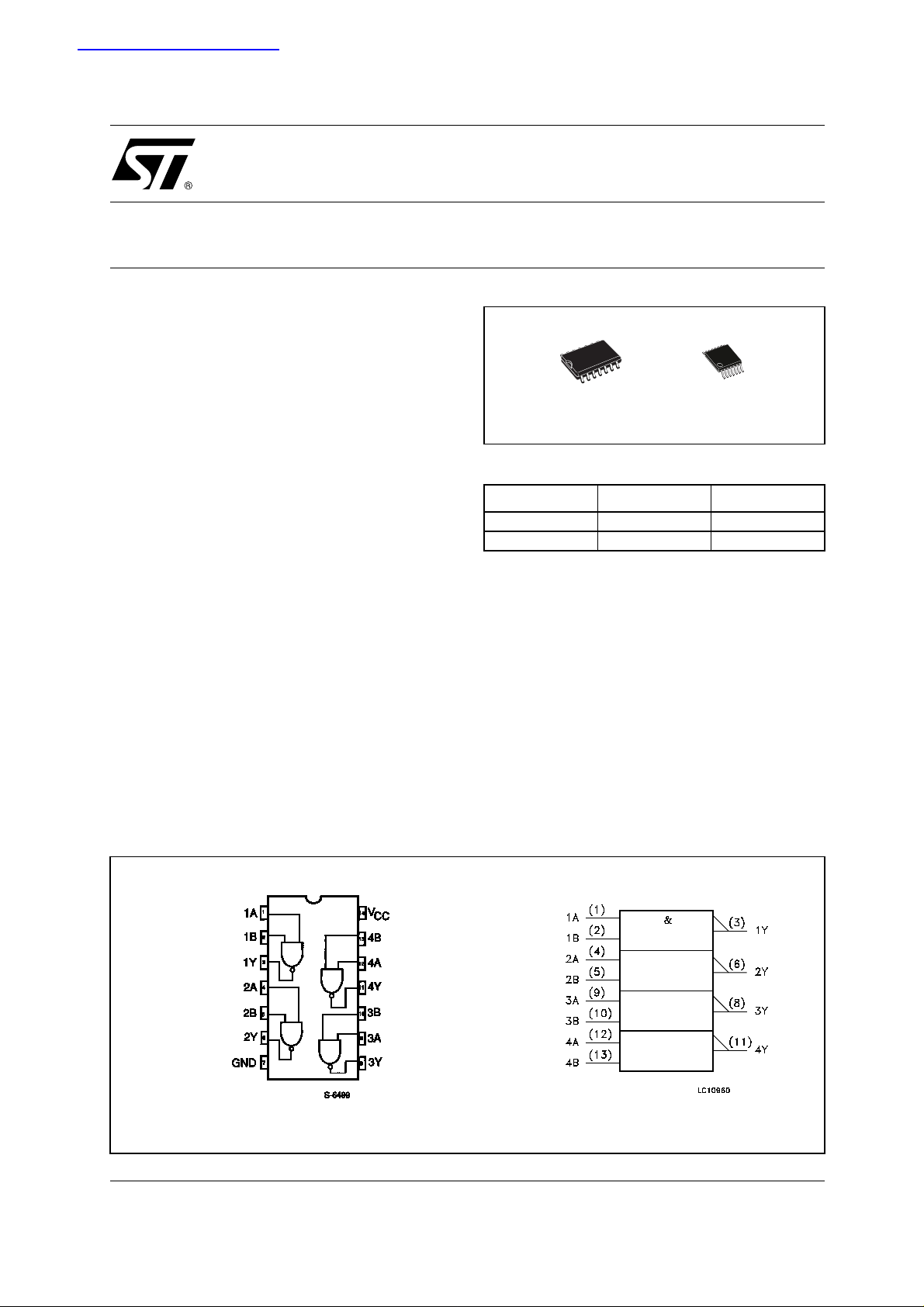
PIN CONNECTION AND IEC LOGIC SYMBOLS
1/8September 2001
74LCX00
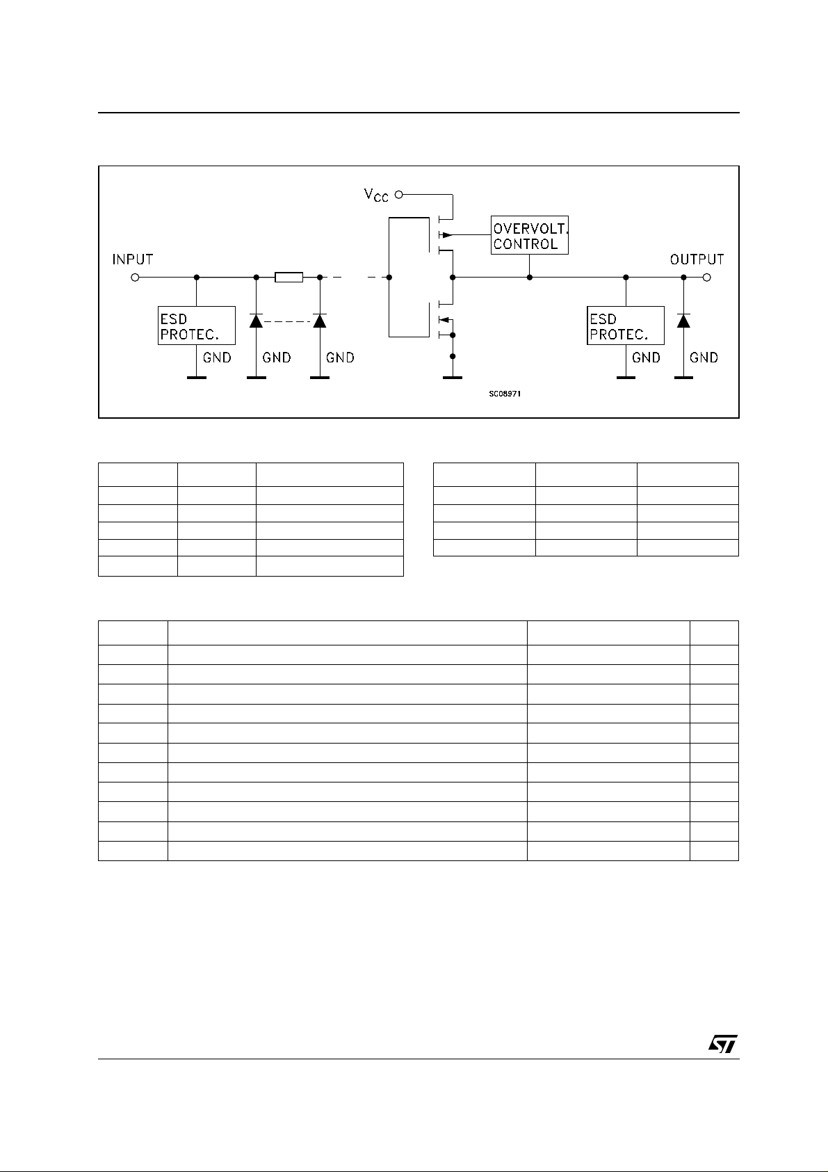
INPUT AND OUTPUT EQUIVALENT CIRCUIT
PIN DESCRIPTION TRUTH TABLE
PIN No SYMBOL NAME AND FUNCTION
1, 4, 9, 12 1A to 4A Data Inputs
2, 5, 10, 13 1B to 4B Data Inputs
3, 6, 8, 11 1Y to 4Y Data Outputs
7 GND Ground (0V)
14
V
CC
Positive Supply Voltage
ABY
LLH
LHH
HLH
HHL
ABSOLUTE MAXIMUM RATINGS
Symbol Parameter Value Unit
V
V
V
V
I
I
OK
I
I
CC
I
GND
T
T
Absolute Maximum Ratings are those values beyond which damage to the device may occur. Functional operation under these conditions is
not implied
1) I
absolute ma xim um rating mu st be observed
O
2) V
< GND
O
Supply Voltage
CC
DC Input Voltage
I
DC Output Voltage (VCC = 0V)
O
DC Output Voltage (High or Low State) (note 1) -0.5 to VCC + 0.5
O
DC Input Diode Current
IK
DC Output Diode Current (note 2)
DC Output Current
O
DC Supply Current per Supply Pin
DC Ground Current per Supply Pin
Storage Temperature
stg
Lead Temperature (10 sec)
L
-0.5 to +7.0 V
-0.5 to +7.0 V
-0.5 to +7.0 V
V
-50 mA
-50 mA
± 50 mA
± 100 mA
± 100 mA
-65 to +150 °C
300 °C
2/8
74LCX00
RECOMMENDED OPERATING CONDITIONS
Symbol Parameter Value Unit
V
V
V
V
I
OH
I
OH
T
dt/dv Input Rise and Fall Time (note 2) 0 to 10 ns/V
1) Truth T abl e guaranteed: 1.5V to 3.6V
from 0.8V to 2V at VCC = 3.0V
2) V
IN
DC SPECIFICATIONS
Supply Voltage (note 1)
CC
Input Voltage
I
Output Voltage (VCC = 0V)
O
Output Voltage (High or Low State) 0 to V
O
, I
High or Low Level Output Current (VCC = 3.0 to 3.6V)
OL
, I
High or Low Level Output Current (VCC = 2.7V)
OL
Operating Temperature
op
Test Condition Value
2.0 to 3.6 V
0 to 5.5 V
0 to 5.5 V
CC
± 24 mA
± 12 mA
-55 to 125 °C
V
Symbol Parameter
IH
IL
OH
OL
I
I
off
CC
High Level Input
Voltage
Low Level Input
Voltage
High Level Output
Voltage
Low Level Output
Voltage
Input Leakage
Current
Power Off Leakage
Current
Quiescent Supply
Current
ICC incr. per Input
V
V
V
V
I
I
CC
∆I
V
CC
(V)
2.7 to 3.6
2.7 to 3.6
2.7
3.0
2.7 to 3.6
2.7
3.0
2.7 to 3.6
0
2.7 to 3.6
2.7 to 3.6
-40 to 85 °C -55 to 125 °C
Min. Max. Min. Max.
2.0 2.0 V
0.8 0.8 V
IO=-100 µAVCC-0.2 VCC-0.2
=-12 mA
I
O
I
=-18 mA
O
I
=-24 mA
O
IO=100 µA
I
=12 mA
O
I
=16 mA
O
I
=24 mA
O
= 0 to 5.5V
V
I
or VO = 5.5V
V
I
VI = VCC or GND
V
or VO= 3.6 to 5.5V
I
VIH = VCC - 0.6V
2.2 2.2
2.4 2.4
2.2 2.2
0.2 0.2
0.4 0.4
0.4 0.4
0.55 0.55
± 5 ± 5 µA
10 10 µA
10 10
± 10 ± 10
500 500 µA
Unit
V
V
µA
DYNAMIC SWITCHING CHARACTERISTICS
Test Condition Value
T
Symbol Parameter
V
OLP
V
OLV
1) Number of outputs d ef i ned as "n". Me asured with "n-1" output s switching from HIGH to LO W or LOW to HIGH. The remaini ng outpu t is
measur ed i n the LOW state.
Dynamic Low Level Quiet
Output (note 1)
V
3.3
CC
(V)
= 50pF
C
L
V
= 0V, VIH = 3.3V
IL
Min. Typ. Max.
= 25 °C
A
0.8
-0.8
Unit
V
3/8
 Loading...