

Features
74AUP1G125
Low power single tristate buffer
■ High speed: t
■ Power down protection on inputs and outputs
■ Balanced propagation delays:
t
≈ t
PLH
■
Operating voltage range:
V
CC
■ Low power dissipation:
I
CC
■ Latch-up performance exceeds 300 mA
PHL
(opr) = 1.2 to 3.6 V
= 1 µA (max.) at TA = 85 °C
= 6.3 ns (max.) at VCC = 2.3 V
PD
(JESD 78, Class II)
■ ESD performance:
– 2000-V human body model (A114-A)
– 200-V machine model (A115-A)
– 1000-V charged device model (C101)
Applications
■ Mobile phones
■ Personal digital assistants (PDAs)
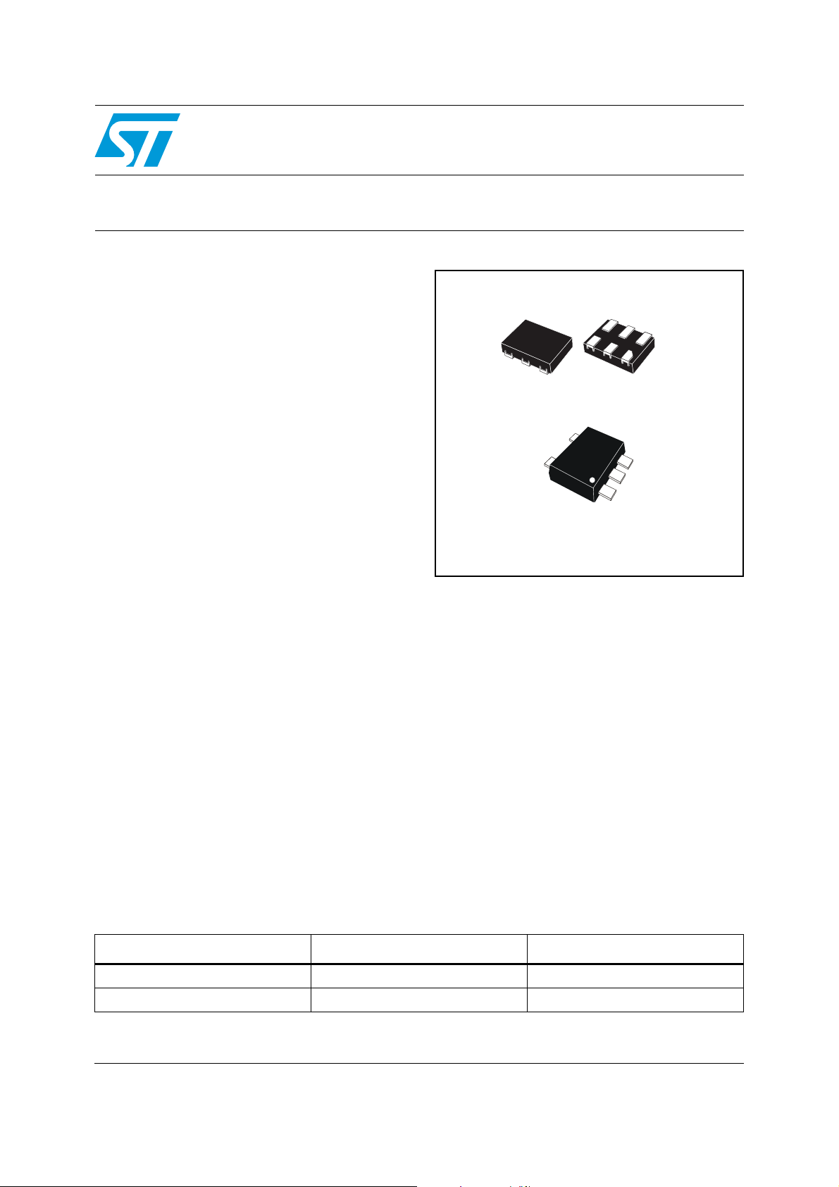
DFN6L
SOT-665
Description
The 74AUP1G125 is a low voltage CMOS single
tristate buffer fabricated with sub-micron silicon
gate and double-layer metal wiring C
technology. It is ideal for 1.2 to 3.6 V operations
and low power and low noise applications.
2
MOS
All inputs and outputs are equipped with
protection circuits against static discharge, giving
them 2 kV ESD immunity and transient excess
voltage.
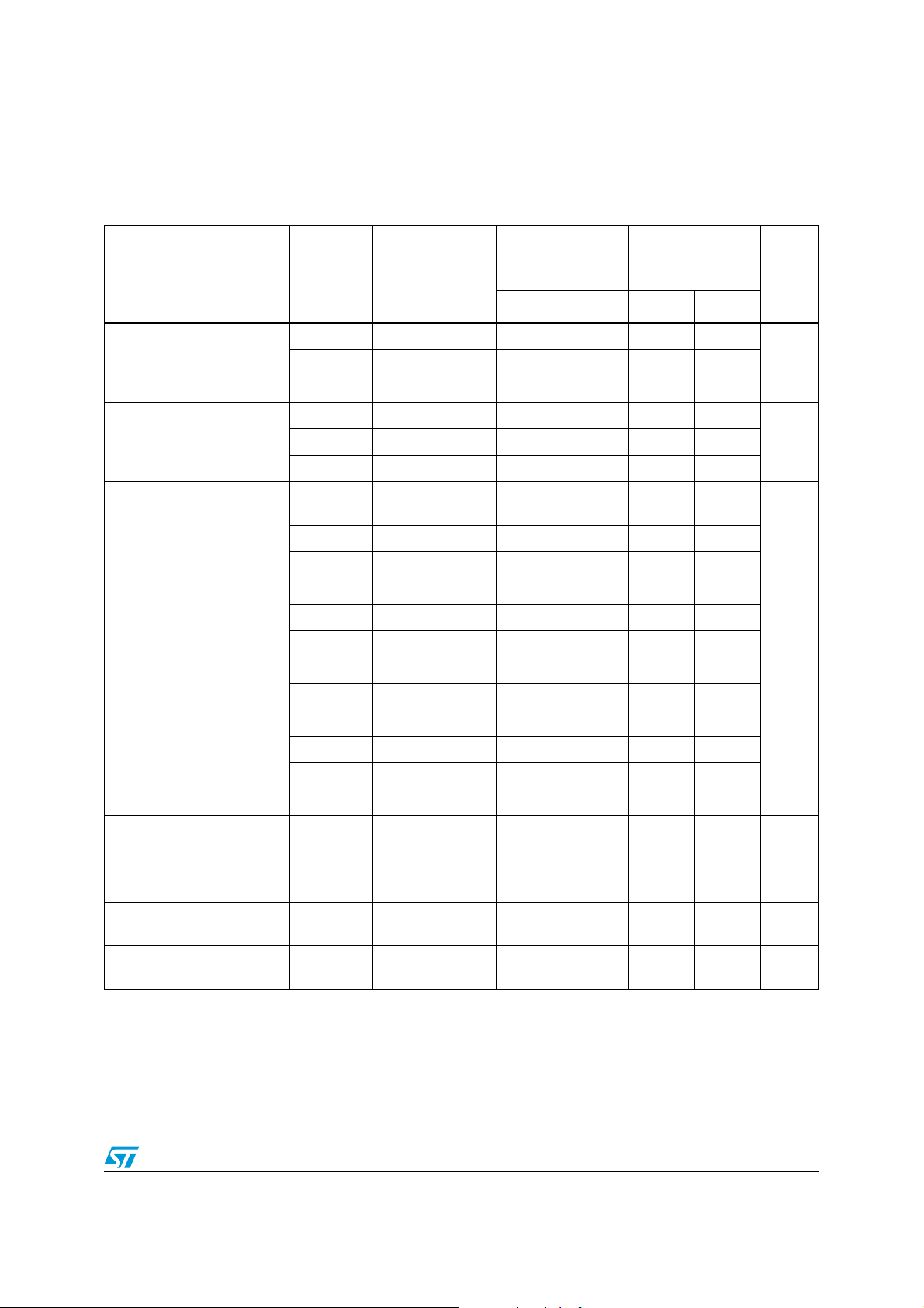
Table 1. Device summary
June 2009 Doc ID 15666 Rev 1 1/20
Order code Package Packing
74AUP1G125DTR DFN6L (1.2 x 1 mm) Tape and reel
74AUP1G125GTR SOT-665 (1.6 x 1.6 mm) Tape and reel
www.st.com
20
Pin settings 74AUP1G125
1 Pin settings
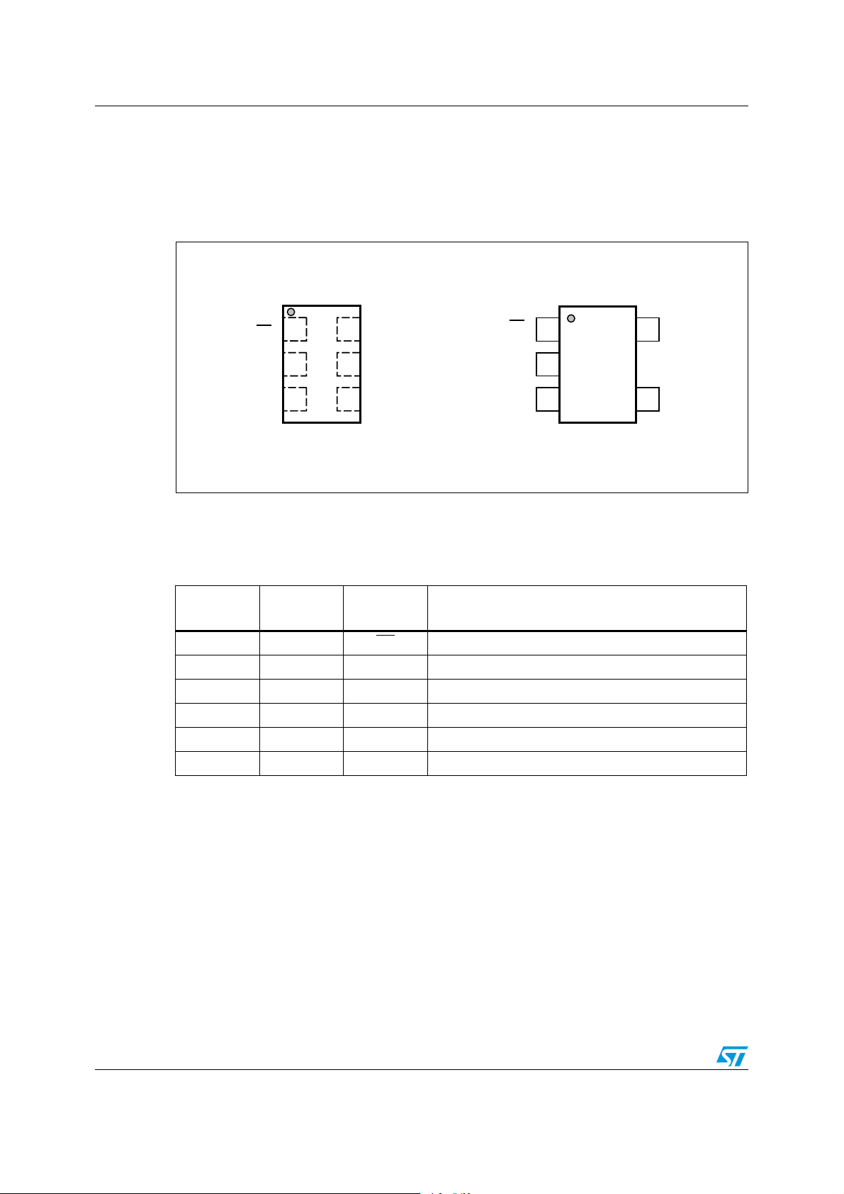
1.1 Pin connection
Figure 1. Pin connection (top through view)
/%
'.$
$&.,
1.2 Pin description
Table 2. Pin assignment
DFN pin
number
11OE
2 2 A Data input
3 3 GND Ground (0V)
4 4 B Data output
5 - NC Not connected
65V
SOT pin
number
6##
"
/%
'.$
3/4
Symbol Name and function
Active low output enable
CC
Positive supply voltage
6##
"
!-6
2/20 Doc ID 15666 Rev 1
74AUP1G125 Pin settings
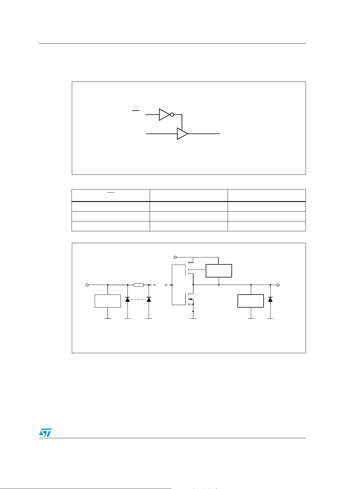
1.3 Truth table
Figure 2. Truth table
/%
!
Table 3. Truth table
OE AB
LLL
LHH
HXZ
Figure 3. Input and output equivalent circuit
V
CC
Input
ESD
protection
"
Overvoltage
control
ESD
protection
!-6
Output
GND GND GND
GND
GND
CS08974
Doc ID 15666 Rev 1 3/20
Maximum rating 74AUP1G125
2 Maximum rating
Stressing the device above the rating listed in the “absolute maximum ratings” table may
cause permanent damage to the device. These are stress ratings only and operation of the
device at these or any other conditions above those indicated in the operating sections of
this specification is not implied. Exposure to absolute maximum rating conditions for
extended periods may affect device reliability.
Table 4. Absolute maximum ratings
Symbol Parameter Value Unit
V
V
V
V
I
I
OK
I
I
CC
I
GND
P
T
T
CC
IK
O
stg
Supply voltage -0.5 to +4.6 V
DC input voltage -0.5 to +4.6 V
I
DC output voltage (VCC = 0 V) -0.5 to +4.6 V
O
DC output voltage (high or low state) -0.5 to VCC + 0.5 V
O
DC input diode current -20 mA
DC output diode current -50 mA
DC output current ±50 mA
DC supply current per supply pin ±100 mA
DC ground current per supply pin ±100 mA
Power dissipation 200 mW
D
Storage temperature -65 to +150 °C
Lead temperature (10 sec) 260 °C
L
2.1 Recommended operating conditions
Table 5. Recommended operating conditions
Symbol Parameter Value Unit
V
CC
V
V
T
op
dt/dv Input rise and fall time
Supply voltage 1.2 to 3.6 V
Input voltage 0 to V
I
Output voltage 0 to V
O
Operating temperature -40 to 85 °C
V
= 3.0 to 3.6 V 10 ns/V
CC
= 2.3 to 2.7 V 20 ns/V
V
CC
= 1.2 to 1.95 V 100 ns/V
V
CC
CC
CC
V
V
4/20 Doc ID 15666 Rev 1
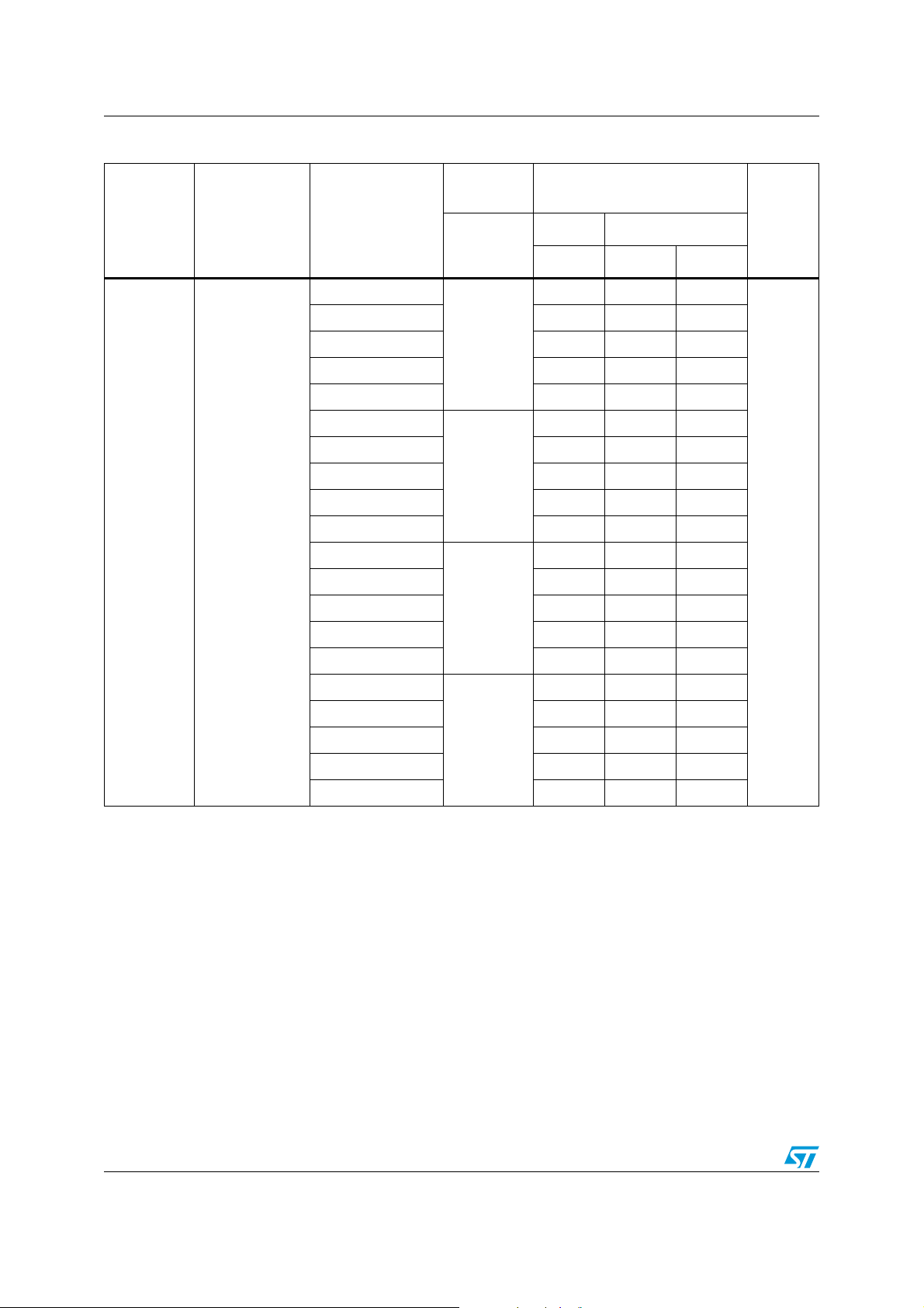
74AUP1G125 Electrical characteristics
3 Electrical characteristics
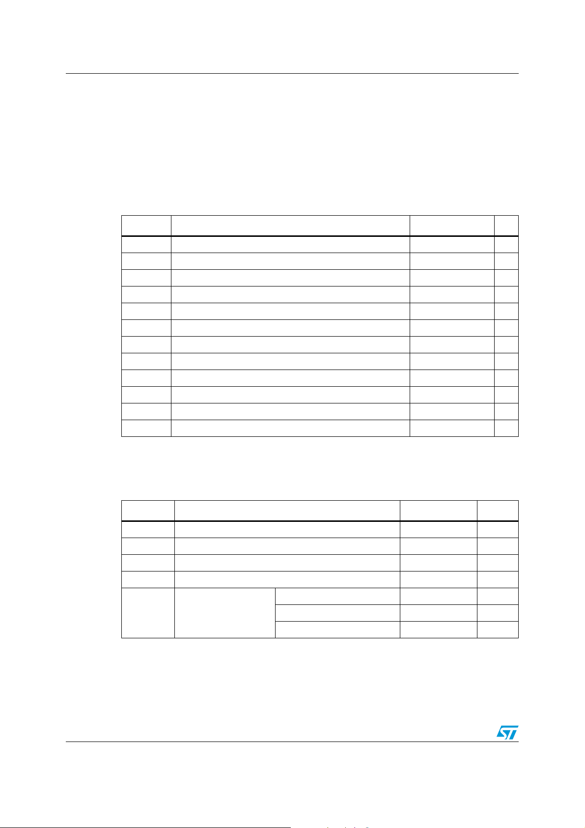
Table 6. DC specifications
Symbol Parameter
1.2 to 1.95 - 0.65 V
IH
High level input
voltage
V
2.75 to 3.6 - 2.0 - 2.0 -
1.2 to 1.95 - - 0.35 V
IL
Low level input
voltage
V
2.75 to 3.6 - - 0.8 0.8
1.2 to 3.6 I
V
OH
High level
output voltage
1.2 to 3.6 I
I
Low level
output voltage
Input leakage
current
0 to 3.6 V
V
OL
I
V
CC
(V)
3.0 I
2.3 I
1.65 I
1.4 I
1.2 I
3.0 I
2.3 I
1.65 I
1.4 I
1.2 I
Val ue Val ue
Test condition
Min Max Min Max
CC
V
= -100 µA
OH
= -10 mA 2.45 - 2.4 -
OH
= -6 mA 1.85 - 1.8 -
OH
= -4 mA 1.30 - 1.25 -
OH
= -2 mA 1.10 - 1.05 -
OH
= -1 mA 1.00 - 0.95 -
OH
= 100 µA - 0.15 - 0.20
O
= 10 mA - 0.50 - 0.55
O
= 6 mA - 0.35 - 0.40
O
= 4 mA - 0.35 - 0.40
O
= 2 mA - 0.25 - 0.30
O
= 1 mA - 0.20 - 0.25
O
= GND to 3.6 - ±0.1 - ±0.5 µA
I
CC –
0.2
-0.65VCC-
CC
-
V
CC –
0.2
0.35V
-
CC
Unit25 °C -40 to 85 °C
V2.0 to 2.7 - 1.6 - 1.6 -
V2.0 to 2.7 - - 0.7 0.7
V
V
CC
Power off
leakage current
Quiescent
supply current
ICC increment
per input
0
1.2 to 3.6 V
3.3
I
off
I
CC
ΔI
VI or VO = 0 to
3.6 V
= VCC or GND - 0.1 - 1 µA
I
VI = VCC - 0.6V,
IO = 0
-±0.1-±1.0µA
-80-100µA
Doc ID 15666 Rev 1 5/20
Electrical characteristics 74AUP1G125
Table 7. AC electrical characteristics
Symbol Parameter
V
CC
(V)
1.1 to 1.3
1.4 to 1.6 3.5 - 5.6
1.65 to 1.95 3.0 - 4.9
2.3 to 2.7 2.9 - 4.0
3.0 to 3.6 2.5 - 3.4
1.1 to 1.3
1.4 to 1.6 3.9 - 6.0
1.65 to 1.95 3.4 - 5.2
2.3 to 2.7 2.8 - 4.1
t
PLH, tPHL
Propagation
delay time
3.0 to 3.6 2.6 - 3.8
1.1 to 1.3
1.4 to 1.6 4.4 - 5.9
1.65 to 1.95 3.8 - 5.8
Tes t
condition
C
(pF)
L
5
10
15
Value
25 °C -40 to 85 °C
Typ Mi n Ma x
5.7 - 8.9
7.0 - 10.6
8.0 - 11.8
Unit
ns
2.3 to 2.7 3.1 - 4.4
3.0 to 3.6 2.9 - 4.2
1.1 to 1.3
10.2 - 15.6
1.4 to 1.6 5.7 - 9.4
1.65 to 1.95 5.3 - 8.3
30
2.3 to 2.7 4.5 - 6.3
3.0 to 3.6 4.2 - 6.0
6/20 Doc ID 15666 Rev 1
 Loading...