

ST 54VCXH162374 User Manual
Rad hard low voltage CMOS 16-bit d-type flip-flop (3-state)
with 3.6 V tolerant inputs and outputs
Features
■ 1.65 to 3.6 V inputs and outputs
■ High speed:
–t
= 3.4 ns (Max.) at V
PD
–t
= 4.8 ns (Max.) at V
PD
■ Symmetrical impedance outputs:
–|I
–|I
■ Power down protection on inputs and outputs
■ 26 Ω serie resistors in outputs
■ Operating voltage range:
–V
■ Pin and function compatible with 54 series
| = IOL = 12 mA (Min.) at VCC = 3.0 V
OH
| = IOL = 8 mA (Min.) at VCC = 2.3 V
OH
(Opr) = 1.65 V to 3.6 V
CC
H162374
■ Bus hold provided on both sides
■ Cold spare function
■ Latch-up performance exceeds
300 mA (JESD 17)
■ ESD performance:
– HBM > 2000 V
(MIL STD 883 method 3015); MM > 200 V
■ 300 KRad Mil1019.6 condition A, (RHA QML
qualification extension undergone)
■ No SEL, no SEU and no SET under 110
Mev/cm2/mg LET heavy ions irradiation
■ QML qualified product
■ Device fully compliant with
DSCC SMD 5962-05212
■ 100 mV typical input hysteresis
= 3.0 to 3.6 V
CC
= 2.3 to 2.7 V
CC
54VCXH162374
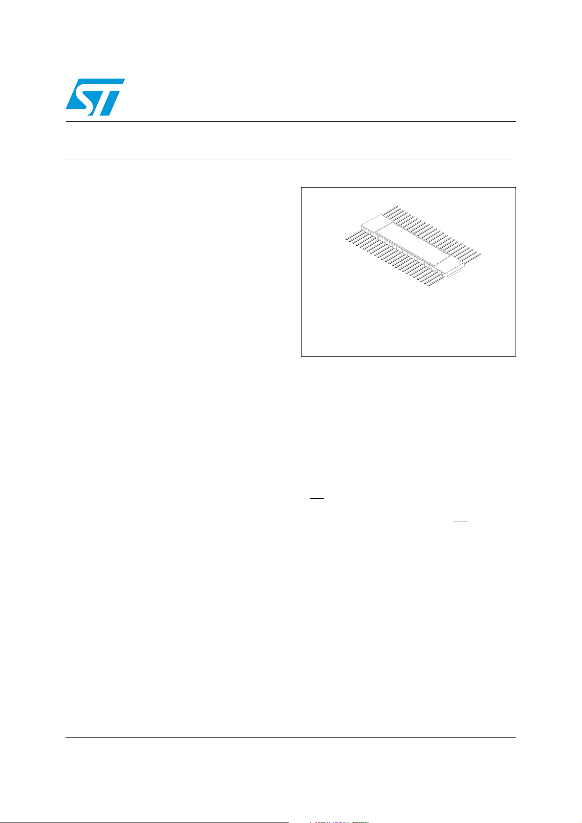
Flat-48
The upper metallic lid is not electrically connected to any
pins, nor to the IC die inside the package.
Description
The 54VCXH162374 is a low voltage CMOS 16
bit d-type flip-flop with 3 state outputs non
inverting fabricated with sub-micron silicon gate
and five-layer metal wiring C²MOS technology. It
is ideal for low power and very high speed 1.65 to
3.6 V applications; it can be interfaced to 3.6 V
signal environment for both inputs and outputs.
These 16 bit d-type flip-flops are controlled by two
clock inputs (nCK) and two output enable inputs
(nOE
). On the positive transition of the (nCK), the
nQ outputs will be set to the logic state that were
setup at the nD inputs. While the (nOE
low, the 8 outputs (nQ) will be in a normal state
(HIGH or LOW logic level) and while high level the
outputs will be in a high impedance state. Any
output control does not affect the internal
operation of flip flops; that is, the old data can be
retained or the new data can be entered even
while the outputs are OFF.
) input is
August 2011 Doc ID 10654 Rev 7 1/18
www.st.com
18

Contents 54VCXH162374
Contents
1 Logic symbols and I/O equivalent circuit . . . . . . . . . . . . . . . . . . . . . . . . 3
2 Pin settings . . . . . . . . . . . . . . . . . . . . . . . . . . . . . . . . . . . . . . . . . . . . . . . . 5
2.1 Pin connection . . . . . . . . . . . . . . . . . . . . . . . . . . . . . . . . . . . . . . . . . . . . . . 5
2.2 Pin description . . . . . . . . . . . . . . . . . . . . . . . . . . . . . . . . . . . . . . . . . . . . . . 6
2.3 Truth table . . . . . . . . . . . . . . . . . . . . . . . . . . . . . . . . . . . . . . . . . . . . . . . . . . 6
3 Maximum rating . . . . . . . . . . . . . . . . . . . . . . . . . . . . . . . . . . . . . . . . . . . . . 7
3.1 Recommended operating conditions . . . . . . . . . . . . . . . . . . . . . . . . . . . . . 7
4 Electrical characteristics . . . . . . . . . . . . . . . . . . . . . . . . . . . . . . . . . . . . . 8
5 Test circuit . . . . . . . . . . . . . . . . . . . . . . . . . . . . . . . . . . . . . . . . . . . . . . . . 11
6 Waveforms . . . . . . . . . . . . . . . . . . . . . . . . . . . . . . . . . . . . . . . . . . . . . . . . 12
7 Package mechanical data . . . . . . . . . . . . . . . . . . . . . . . . . . . . . . . . . . . . 14
8 Order codes . . . . . . . . . . . . . . . . . . . . . . . . . . . . . . . . . . . . . . . . . . . . . . . 16
9 Revision history . . . . . . . . . . . . . . . . . . . . . . . . . . . . . . . . . . . . . . . . . . . 17
2/18 Doc ID 10654 Rev 7
54VCXH162374 Logic symbols and I/O equivalent circuit
1 Logic symbols and I/O equivalent circuit
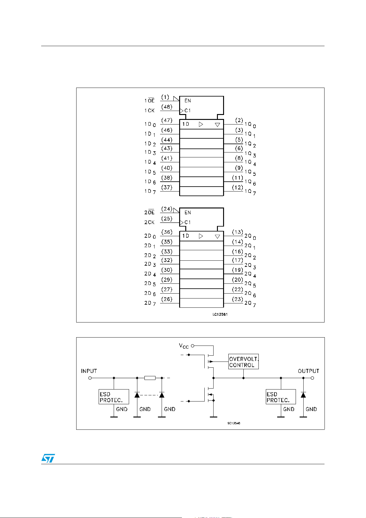
Figure 1. IEC logic symbols
Figure 2. Input and output equivalent circuit
Doc ID 10654 Rev 7 3/18
Logic symbols and I/O equivalent circuit 54VCXH162374
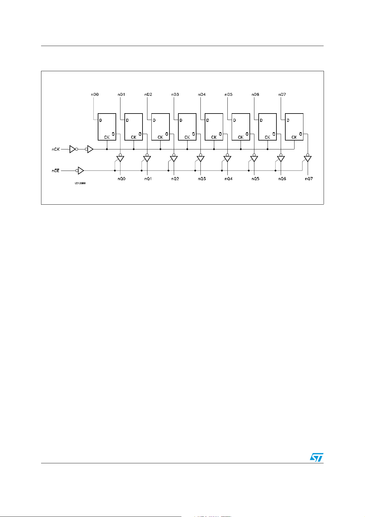
Figure 3. Logic diagram
Note: This logic diagram has not to be used to estimate propagation delays
4/18 Doc ID 10654 Rev 7
54VCXH162374 Pin settings
2 Pin settings
2.1 Pin connection
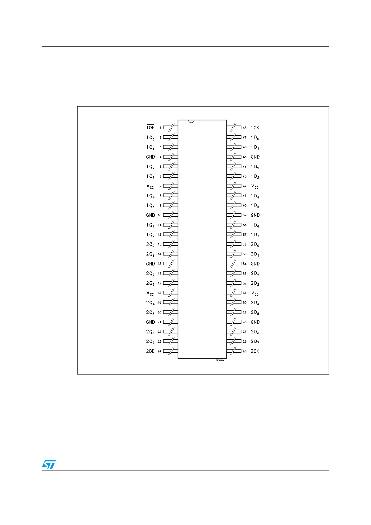
Figure 4. Pin connection (top through view)
Doc ID 10654 Rev 7 5/18
Pin settings 54VCXH162374
2.2 Pin description
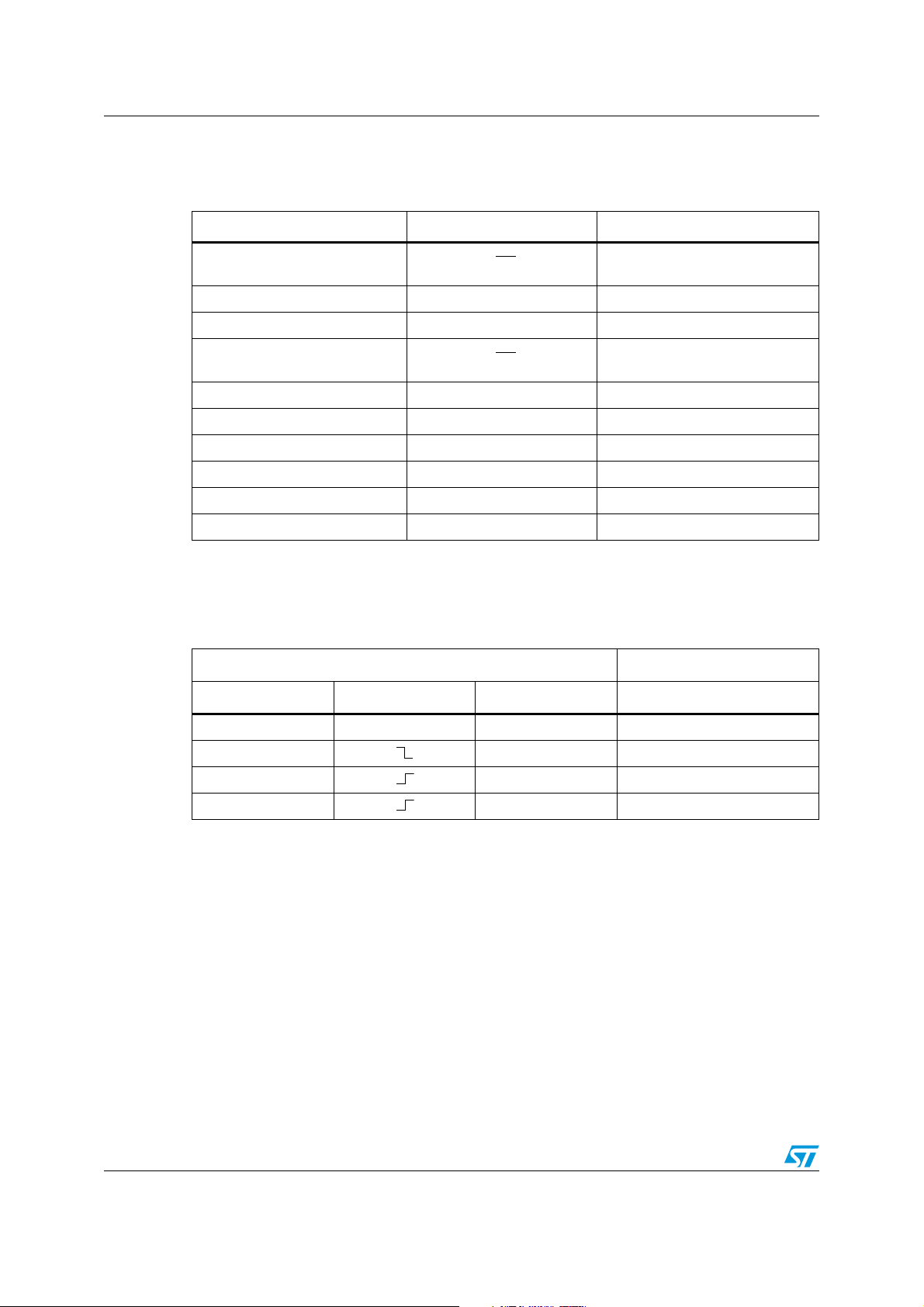
Table 1. Pin description
Pin n° Symbol Name and function
2, 3, 5, 6, 8, 9, 11, 12 1Q0 to 1Q7 3-state outputs
13, 14, 16, 17, 19, 20, 22, 23 2Q0 to 2Q7 3-state outputs
36, 35, 33, 32, 30, 29, 27, 26 2D0 to 2D7 Data inputs
47, 46, 44, 43, 41, 40, 38, 37 1D0 to 1D7 Data inputs
4, 10, 15, 21, 28, 34, 39, 45 GND Ground (0 V)
7, 18, 31, 42 V
2.3 Truth table
Table 2. Truth table
OE LE D Q
11OE
24 2OE
3 state output enable input
(Active LOW)
3 state output enable input
(Active LOW)
25 2CK Clock input
48 1CK Clock input
CC
Positive supply voltage
Inputs Output
HXX Z
L X No change
LLL
LHH
1. Q outputs are latched at the time when the LE input is taken low logic level.
Note: X = Do not care; Z = High impedance
6/18 Doc ID 10654 Rev 7
(1)
 Loading...