

ST 54VCXH162373 User Manual
Rad hard low voltage CMOS 16-bit D-type latch (3-state)
Features
■ 1.65 to 3.6 V inputs and outputs
■ High speed:
–t
= 3.3 ns (Max.) at V
PD
–t
= 4.5 ns (Max.) at V
PD
■ Symmetrical impedance outputs:
–|I
–|I
■ Power down protection on inputs and outputs
■ 26 Ω serie resistors in outputs
■ Operating voltage range:
–V
■ Pin and function compatible with 54 series
| = IOL = 12 mA (Min.) at VCC = 3.0 V
OH
| = IOL = 8 mA (Min.) at VCC = 2.3 V
OH
(Opr) = 1.65 V to 3.6 V
CC
HR162373
■ Bus hold provided on both sides
■ Cold spare function
■ Latch-up performance exceeds
300 mA (JESD 17)
■ ESD performance:
– HBM > 2000 V
(MIL STD 883 method 3015); MM > 200 V
■ 300 krad Mil1019.6 condition A, (RHA QML
qualification extension undergone)
■ No SEL, no SEUand no SET under 110
Mev/cm2/mg LET heavy ions irradiation
■ QML qualified product
■ Device fully compliant with
DSCC SMD 5962-05211
■ 100 mV typical input hysteresis
= 3.0 to 3.6 V
CC
= 2.3 to 2.7 V
CC
54VCXH162373
with 3.6 V tolerant inputs and outputs
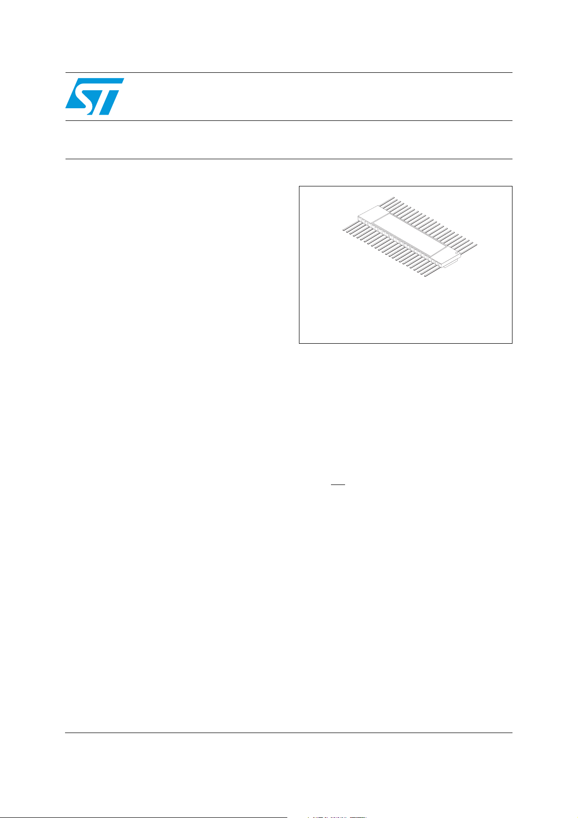
Flat-48
The upper metallic lid is not electrically connected to any
pins, nor to the IC die inside the package.
Description
The 54VCXH162373 is a low voltage CMOS 16
bit d-type latch with 3 state outputs non inverting
fabricated with sub-micron silicon gate and fivelayer metal wiring C²MOS technology. It is ideal
for low power and very high speed 1.65 to 3.6 V
applications; it can be interfaced to 3.6 V signal
environment for both inputs and outputs. These
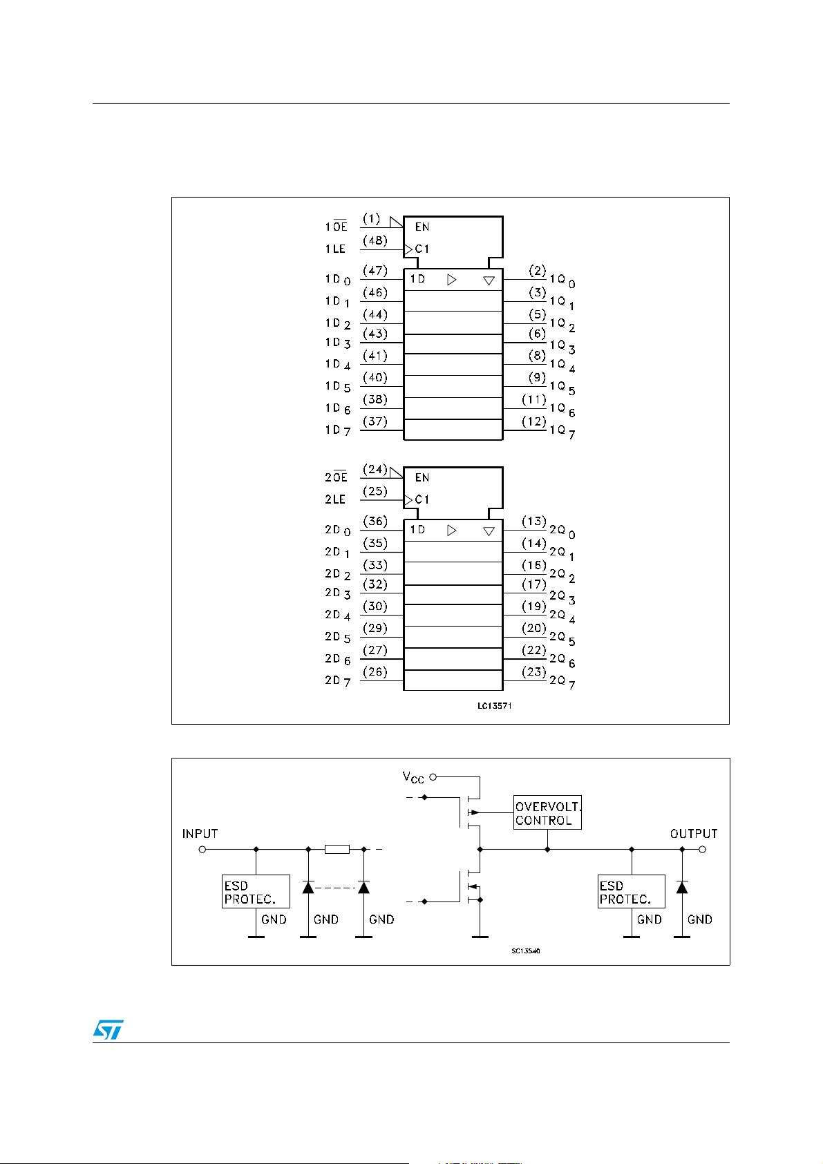
16 bit D-type latches are bite controlled by two
latch enable inputs (nLE) and two output enable
inputs (OE
level, the nQ outputs will follow the data input
precisely. When the nLE is taken low, the nQ
outputs will be in a normal logic state (high or low
logic level) and while high level the outputs will be
in a high impedance state. Bus hold on data
inputs is provided in order to eliminate the need
for external pull-up or pull-down resistor. The
device circuits is including 26 Ω series resistance
in the outputs. These resistors permit to reduce
line noise in high speed applications. All inputs
and outputs are equipped with protection circuits
against static discharge, giving them 2 kV ESD
immunity and transient excess voltage.
). While the nLE input is held at a high
August 2011 Doc ID 10653 Rev 7 1/18
www.st.com
18

Contents 54VCXH162373
Contents
1 Logic symbols and I/O equivalent circuit . . . . . . . . . . . . . . . . . . . . . . . . 3
2 Pin settings . . . . . . . . . . . . . . . . . . . . . . . . . . . . . . . . . . . . . . . . . . . . . . . . 5
2.1 Pin connection . . . . . . . . . . . . . . . . . . . . . . . . . . . . . . . . . . . . . . . . . . . . . . 5
2.2 Pin description . . . . . . . . . . . . . . . . . . . . . . . . . . . . . . . . . . . . . . . . . . . . . . 6
2.3 Truth table . . . . . . . . . . . . . . . . . . . . . . . . . . . . . . . . . . . . . . . . . . . . . . . . . . 6
3 Maximum rating . . . . . . . . . . . . . . . . . . . . . . . . . . . . . . . . . . . . . . . . . . . . . 7
3.1 Recommended operating conditions . . . . . . . . . . . . . . . . . . . . . . . . . . . . . 7
4 Electrical characteristics . . . . . . . . . . . . . . . . . . . . . . . . . . . . . . . . . . . . . 8
5 Test circuit . . . . . . . . . . . . . . . . . . . . . . . . . . . . . . . . . . . . . . . . . . . . . . . . 11
6 Waveforms . . . . . . . . . . . . . . . . . . . . . . . . . . . . . . . . . . . . . . . . . . . . . . . . 12
7 Package mechanical data . . . . . . . . . . . . . . . . . . . . . . . . . . . . . . . . . . . . 14
8 Order codes . . . . . . . . . . . . . . . . . . . . . . . . . . . . . . . . . . . . . . . . . . . . . . . 16
9 Revision history . . . . . . . . . . . . . . . . . . . . . . . . . . . . . . . . . . . . . . . . . . . 17
2/18 Doc ID 10653 Rev 7
54VCXH162373 Logic symbols and I/O equivalent circuit
1 Logic symbols and I/O equivalent circuit
Figure 1. IEC logic symbols
Figure 2. Input and output equivalent circuit
Doc ID 10653 Rev 7 3/18
Logic symbols and I/O equivalent circuit 54VCXH162373
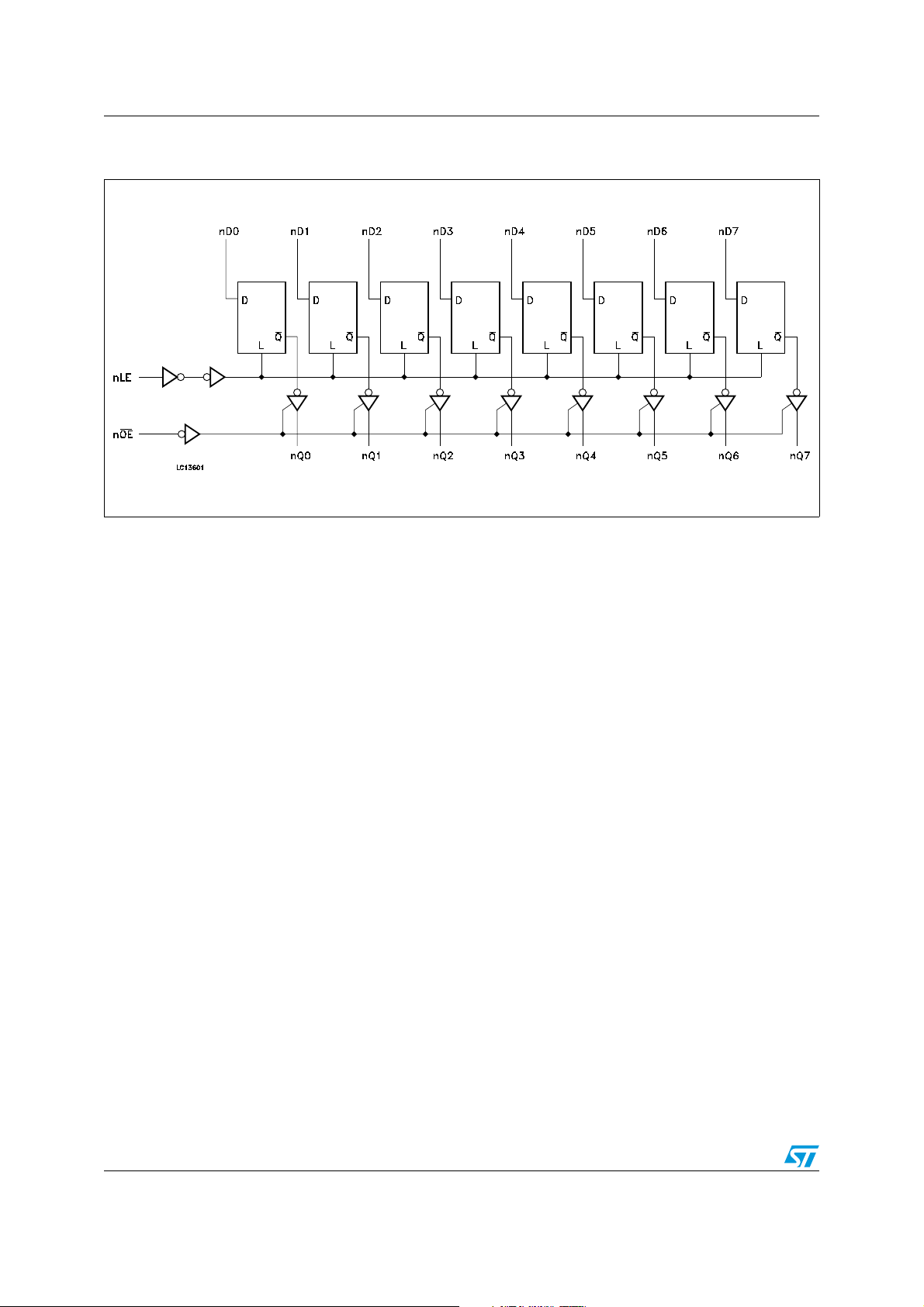
Figure 3. Logic diagram
Note: This logic diagram has not to be used to estimate propagation delays
4/18 Doc ID 10653 Rev 7
54VCXH162373 Pin settings
2 Pin settings
2.1 Pin connection
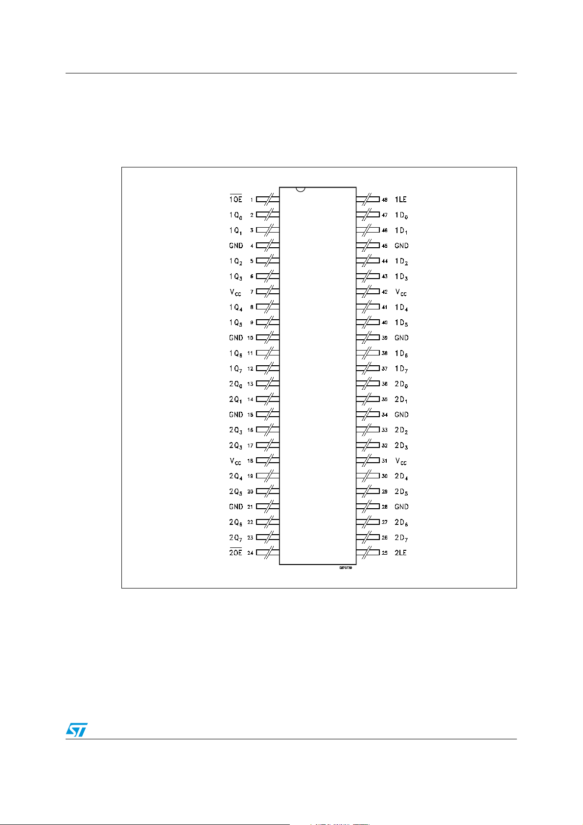
Figure 4. Pin connection (top through view)
Doc ID 10653 Rev 7 5/18
Pin settings 54VCXH162373
2.2 Pin description
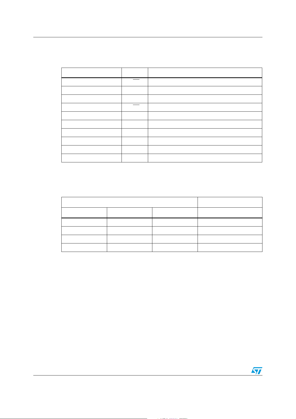
Table 1. Pin description
Pin n° Symbol Name and function
11OE3 state output enable input (active LOW)
2, 3, 5, 6, 8, 9, 11, 12 1Q0 to 1Q7 3-state outputs
13, 14, 16, 17, 19, 20, 22, 23 2Q0 to 2Q7 3-state outputs
24 2OE
25 2LE Latch enable input
36, 35, 33, 32, 30, 29, 27, 26 2D0 to 2D7 Data inputs
47, 46, 44, 43, 41, 40, 38, 37 1D0 to 1D7 Data inputs
48 1LE Latch enable input
4, 10, 15, 21, 28, 34, 39, 45 GND Ground (0 V)
7, 18, 31, 42 V
CC
3 state output enable input (active LOW)
Positive supply voltage
2.3 Truth table
Table 2. Truth table
Inputs Output
OE LE D Q
HXX Z
L L X No change
LHL L
LHH H
1. Q outputs are latched at the time when the LE input is taken low logic level.
Note: X = Do not care; Z = High impedance
(1)
6/18 Doc ID 10653 Rev 7
 Loading...