

ST 54VCXH162244 User Manual
Low voltage CMOS 16-bit bus buffer (3-state non inverter)
with 3.6 V tolerant inputs and outputs
Features
■ 1.65 to 3.6 V inputs and outputs
■ High speed:
–t
= 3.4 ns at V
PD
–t
= 3.8 ns at V
PD
■ Power down protection on inputs and outputs
■ Symmetrical output impedance:
–|I
–|I
■ 26 Ω serie resistors in outputs
■ Operating voltage range:
–V
■ Pin and function compatible with 54 series
| = IOL = 12 mA (Min.) at VCC = 3.0 V
OH
| = IOL = 8 mA (Min.) at VCC = 2.3 V
OH
(Opr) = 1.65 V to 3.6 V
CC
H162244
■ Bus hold provided on data inputs
■ Cold spare function
■ Latch-up performance exceeds
300 mA (JESD 17)
■ ESD performance:
– HBM > 2000 V
(Mil Std 883 Method 3015); MM > 200 V
■ 300 krad Mil1019.6 condition A, (RHA QML
qualification extension undergone)
■ No SEL, no SEU and no SET under 110
Mev/cm2/mg LET heavy ions irradiation
■ QML qualified product
■ SMD 5962-05210
■ 100 mV typical input hysteresis
= 3.0 to 3.6 V
CC
= 2.3 to 2.7 V
CC
54VCXH162244
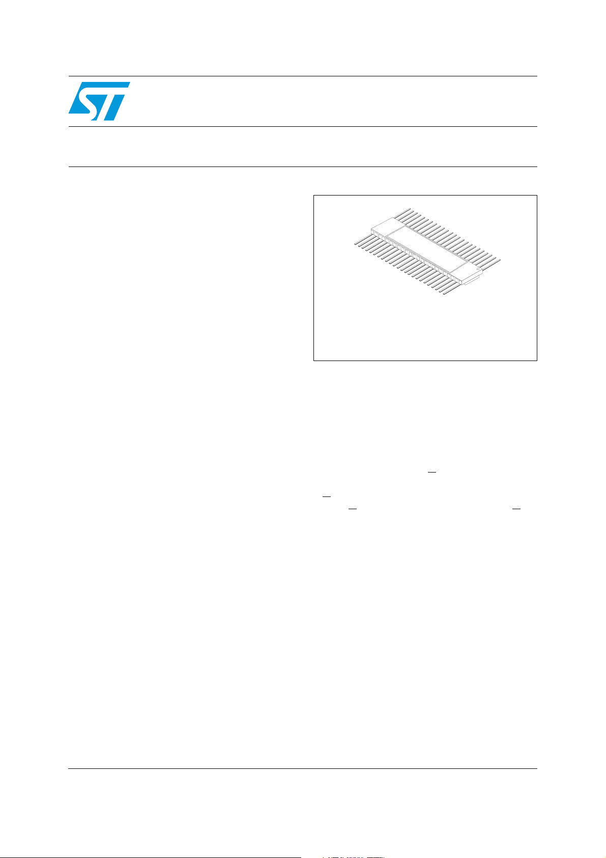
Flat-48
The upper metallic lid is not electrically connected to any
pins, nor to the IC die inside the package.
Description
The 54VCXH162244 is a low voltage CMOS 16
bit bus buffer (non inverted) fabricated with submicron silicon gate and five-layer metal wiring
C²MOS technology. It is ideal for low power and
very high speed 1.65 to 3.6 V applications; it can
be interfaced to 3.6 V signal environment for both
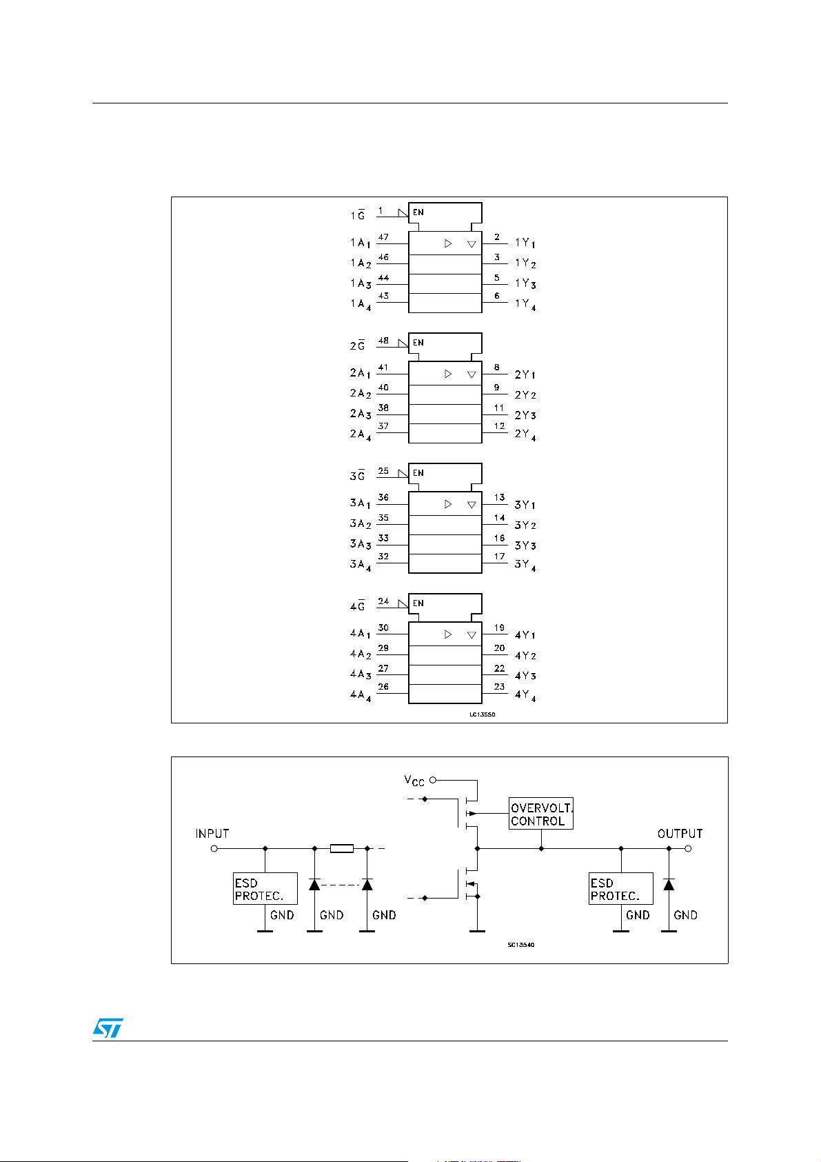
inputs and outputs. Any nG
governs four BUS buffers. Output enable input
(nG
) tied together gives full 16-bit operation.
When nG
is low, the outputs are on. When nG is
high, the output are in high impedance state. This
device is designed to be used with 3 state
memory address drivers, etc. Bus hold on data
inputs is provided in order to eliminate the need
for external pull-up or pull-down resistor. The
device circuits is including 26 Ω series resistance
in the outputs. These resistors permit to reduce
line noise in high speed applications. All inputs
and outputs are equipped with protection circuits
against static discharge, giving them 2 kV ESD
immunity and transient excess voltage.
output control
July 2011 Doc ID 10652 Rev 9 1/18
www.st.com
18

Contents 54VCXH162244
Contents
1 Logic symbols and I/O equivalent circuit . . . . . . . . . . . . . . . . . . . . . . . . 3
2 Pin settings . . . . . . . . . . . . . . . . . . . . . . . . . . . . . . . . . . . . . . . . . . . . . . . . 4
2.1 Pin connection . . . . . . . . . . . . . . . . . . . . . . . . . . . . . . . . . . . . . . . . . . . . . . 4
2.2 Pin description . . . . . . . . . . . . . . . . . . . . . . . . . . . . . . . . . . . . . . . . . . . . . . 5
2.3 Truth table . . . . . . . . . . . . . . . . . . . . . . . . . . . . . . . . . . . . . . . . . . . . . . . . . . 5
3 Maximum rating . . . . . . . . . . . . . . . . . . . . . . . . . . . . . . . . . . . . . . . . . . . . . 6
3.1 Recommended operating conditions . . . . . . . . . . . . . . . . . . . . . . . . . . . . . 6
4 Electrical characteristics . . . . . . . . . . . . . . . . . . . . . . . . . . . . . . . . . . . . . 7
5 Test circuit . . . . . . . . . . . . . . . . . . . . . . . . . . . . . . . . . . . . . . . . . . . . . . . . 11
6 Waveforms . . . . . . . . . . . . . . . . . . . . . . . . . . . . . . . . . . . . . . . . . . . . . . . . 12
7 Package mechanical data . . . . . . . . . . . . . . . . . . . . . . . . . . . . . . . . . . . . 14
8 Order codes . . . . . . . . . . . . . . . . . . . . . . . . . . . . . . . . . . . . . . . . . . . . . . . 16
9 Revision history . . . . . . . . . . . . . . . . . . . . . . . . . . . . . . . . . . . . . . . . . . . 17
2/18 Doc ID 10652 Rev 9
54VCXH162244 Logic symbols and I/O equivalent circuit
1 Logic symbols and I/O equivalent circuit
Figure 1. IEC logic symbols
Figure 2. Input and output equivalent circuit
Doc ID 10652 Rev 9 3/18
Pin settings 54VCXH162244
2 Pin settings
2.1 Pin connection
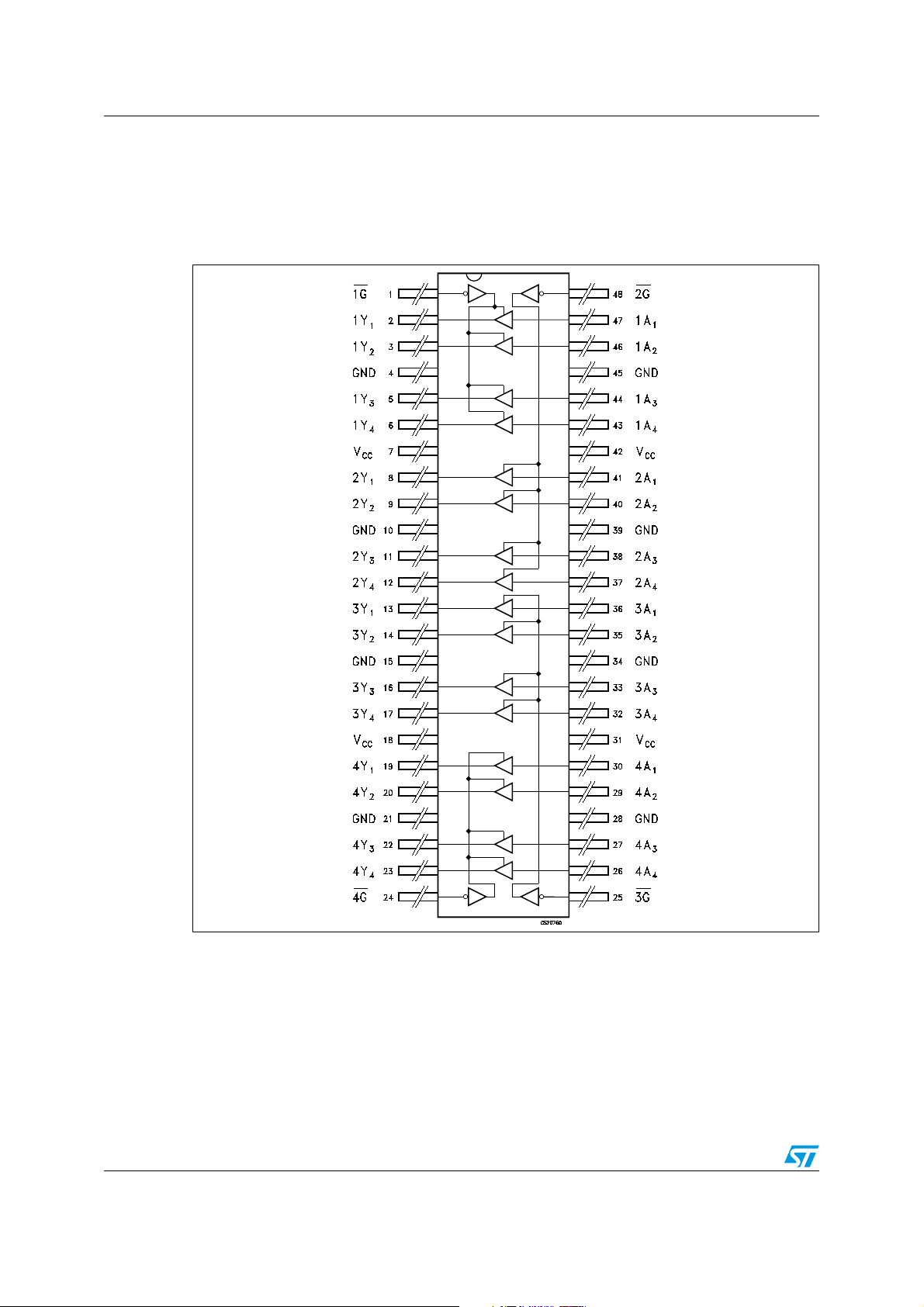
Figure 3. Pin connection (top through view)
4/18 Doc ID 10652 Rev 9
54VCXH162244 Pin settings
2.2 Pin description
Table 1. Pin description
Pin n° Symbol Name and function
11GOutput enable input
2, 3, 5, 6 1Y1 to 1Y4 Data outputs
8, 9, 11, 12 2Y1 to 2Y4 Data outputs
13, 14, 16, 17 3Y1 to 3Y4 Data outputs
19, 20, 22, 23 4Y1 to 4Y4 Data outputs
30, 29, 27, 26 4A1 to 4A4 Data outputs
36, 35, 33, 32 3A1 to 3A4 Data outputs
41, 40, 38, 37 2A1 to 2A4 Data outputs
47, 46, 44, 43 1A1 to 1A4 Data outputs
4, 10, 15, 21, 28, 34, 39, 45 GND Ground (0 V)
7, 18, 31, 42 V
2.3 Truth table
Table 2. Truth table
24 4G
25 3G
48 2G
CC
Output enable input
Output enable input
Output enable Input
Positive supply voltage
Inputs Output
GAnYn
LLL
LHH
HXZ
Note: X = Do not care; Z = High impedance
Doc ID 10652 Rev 9 5/18
Maximum rating 54VCXH162244
3 Maximum rating
Stressing the device above the rating listed in the “absolute maximum ratings” table may
cause permanent damage to the device. These are stress ratings only and operation of the
device at these or any other conditions above those indicated in the operating sections of
this specification is not implied. Exposure to absolute maximum rating conditions for
extended periods may affect device reliability.
Table 3. Absolute maximum ratings
Symbol Parameter Value Unit
I
CC
I
V
V
V
I
I
GND
P
T
T
Supply voltage -0.5 to +4.6 V
CC
DC input voltage -0.5 to +4.6 V
V
I
DC output voltage (OFF state) -0.5 to +4.6 V
O
DC output voltage (high or low state)
O
DC input diode current - 50 mA
IK
DC output diode current
OK
DC output current ± 50 mA
I
O
or
DC VCC or ground current per supply pin ± 100 mA
Power dissipation 400 mW
D
Storage temperature -65 to +150 °C
stg
Lead temperature (10 sec) 260 °C
L
(2)
(1)
1. IO absolute maximum rating must be observed
2. VO < GND, VO > V
CC
3.1 Recommended operating conditions
Table 4. Recommended operating conditions
-0.5 to VCC + 0.5 V
- 50 mA
Symbol Parameter Value Unit
V
V
V
I
OH
I
OH
T
dt/dv Input rise and fall time
1. VIN from 0.8 V to 2 V at VCC = 3.0 V
Supply voltage 1.8 to 3.6 V
CC
Input voltage -0.3 to 3.6 V
V
I
Output voltage (OFF state) 0 to 3.6 V
O
Output voltage (high or low state) 0 to V
O
, I
High or low level output current (VCC = 3.0 to 3.6 V) ± 12 mA
OL
, I
High or low level output current (VCC = 2.3 to 2.7 V) ± 8mA
OL
Operating temperature -55 to 125 °C
op
(1)
6/18 Doc ID 10652 Rev 9
CC
V
0 to 10 ns/V
 Loading...