How it Works
Log In / Sign Up
Buy Points
How it Works
FAQ
Contact Us
Questions and Suggestions
Users
ST
Loading...
#
1.5KE18A
1.5KE200A
1.5KE220A
1.5KE22A
1.5KE24A
1.5KE250A
1.5KE27A
1.5KE300A
1.5KE30A
1.5KE33A
1.5KE350A
1.5KE36A
1.5KE39A
1.5KE400A
1.5KE440A
1.5KE47A
1.5KE56A
1.5KE62A
1.5KE68A
1.5KE6V8A
1.5KE7V5A
1.5KE82A
1N 5333 B
1N 5388 B
1N5711
1N5806U
1N5811U
1N5817
1N5818
1N5819
1N582x
1N6263
1N6640U
1N6642U
2N2219AHR
2N2222AHR
2N2484HR
2N2905AHR
2N2907AHR
2N3019HR
2N3700HR
2N3810HR
2N5153HR
2N5154HR
2N5401HR
2N5551HR
2ST3360
32F401CDISCOVERY
32L100CDISCOVERY
405Q-600
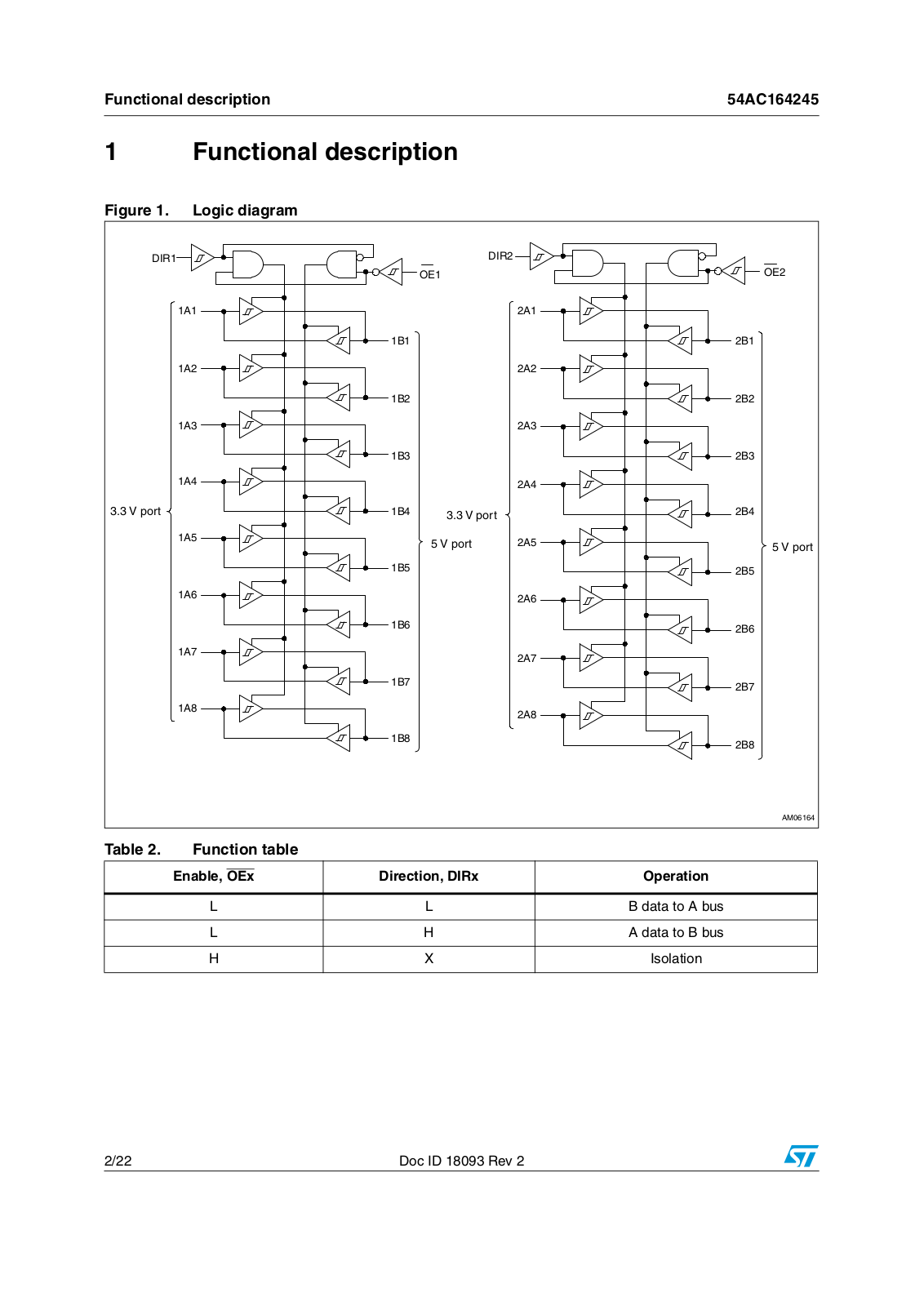
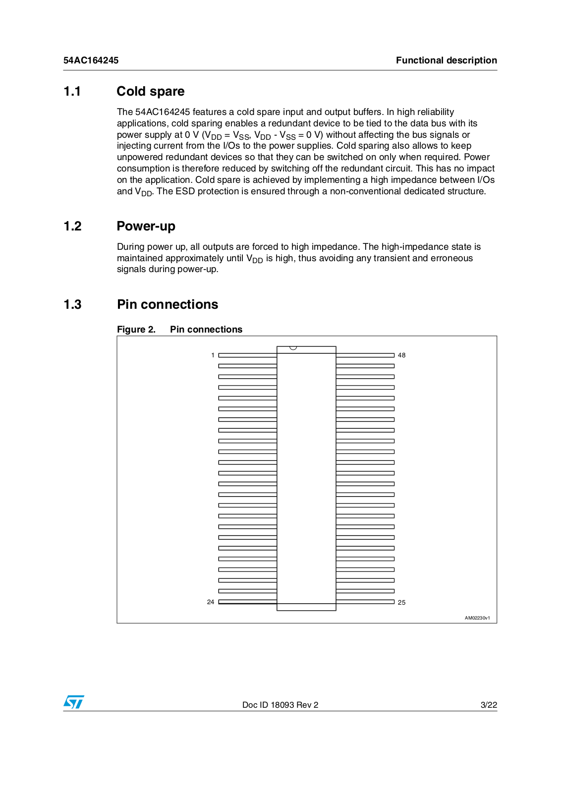
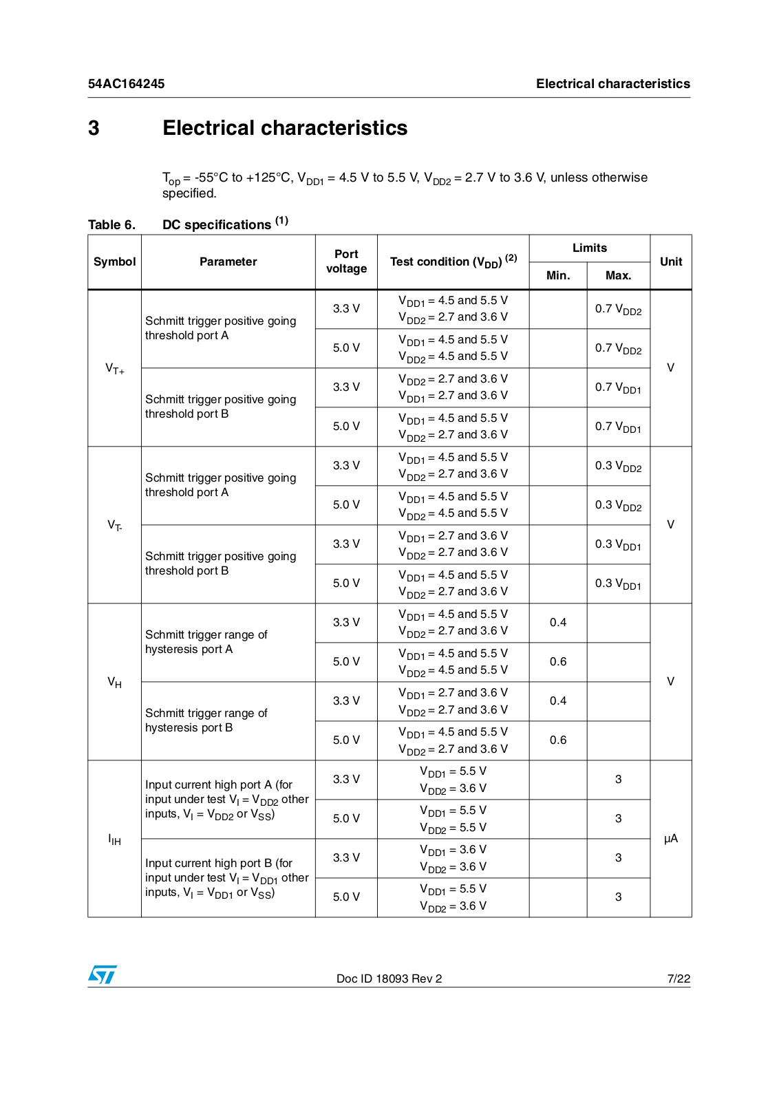
54AC164245
54VCXH162244
54VCXH162245
54VCXH162373
54VCXH162374
54VCXH163245
54VCXHR162245
74AUP1G04
74AUP1G125
74AUP1G32
74H1G66
2
74LCX00
74LCX02
2
74LCX04
2
74LCX05
74LCX07
2
74LCX08
74LCX125
74LCX138
2
74LCX139
2
74LCX14
2
74LCX157
74LCX162244
74LCX16240A
74LCX16244A
74LCX16245
74LCX245
74LCX257
74LCX32
74LCX373M
74LCX374
74LCX541
74LCX573
74LCX74
74LCX86
74LVC00A
74LVC04A
74LVC08A
74LVC125A
74LVC14A
74LVC161284
74LVC244A
74LVC245A
74LVC32A
74LVC373A
74LVC374A
74LVC573A
74LVQ280
74LVQ74
74LVX00
Loading...
Loading...
Nothing found
54AC164245
User Manual
22 pgs
286.39 Kb
0
Table of contents
Loading...
ST 54AC164245 User Manual
...
ST User Manual
Download
Specifications and Main Features
Frequently Asked Questions
User Manual
Download
Loading...
+
15
hidden pages
Unhide
You need points to download manuals.
1 point = 1 manual.
You can buy points or you can get point for every manual you upload.
Buy points
Upload your manuals
 Loading...