

2N5551HR
Hi-Rel NPN bipolar transistor 160 V - 0.5 A
Features
BV
CEO
(max) 0.5 A
I
C
H
at 5 V - 10 mA > 80
FE
160 V
Operating temperature range -65°C to +200°C
■ Linear gain characteristics
■ ESCC qualified
■ European preferred part list - EPPL
■ 100 krad low dose rate
■ Hermetic packages
Description
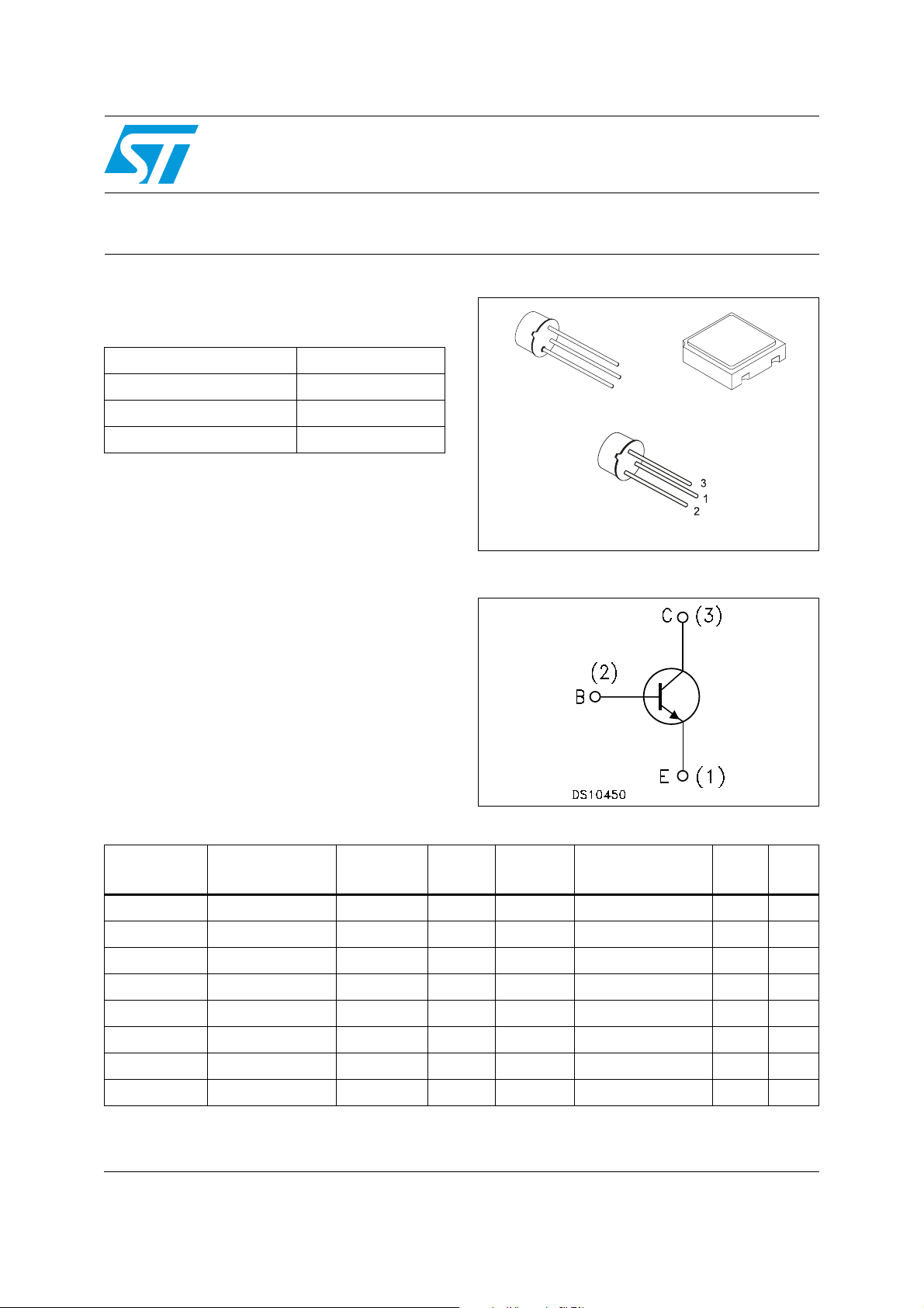
The 2N5551HR is a silicon planar epitaxial NPN
transistor in TO-18, TO-39 and LCC-3 packages.
It is specifically designed for aerospace Hi-Rel
applications and ESCC qualified according to the
5201-019 specification. In case of conflict
between this datasheet and ESCC detailed
specification, the latter prevails.
3
1
2
3
2
TO-18 LCC-3
TO-39
Figure 1. Internal schematic diagram
1
Rad.
level
Packages Lead Finish
Mass
(g)
EPPL
Table 1. Device summary
Order codes
ESCC Part
number
Qual. Level
2N5551UB1 - Eng. Model LCC-3UB Gold 0.06 -
(1)
2N5551UB 5201/019/08 or 09 ESCC Flight LCC-3UB Gold / Solder Dip
0.06 -
SOC5551 - Eng. Model LCC-3 Gold 0.06 -
SOC5551HRB 5201/019/04 or 05 ESCC Flight LCC-3 Gold / Solder Dip
(1)
0.06 Y
SOC5551SW 5201/019/05 ESCC Flight 100 krad LCC-3 Solder Dip 0.06 Y
2N5551/T1 - Eng. Model TO-18 Gold 0.40 -
(1)
(1)
0.40 -
1.20 -
2N5551HR 5201/019/01 or 02 ESCC Flight TO-18 Gold / Solder Dip
2N5551SHR 5201/019/06 or 07 ESCC Flight TO-39 Gold / Solder Dip
1. Depending ESCC part number mentioned on the purchase order.
July 2010 Doc ID 16935 Rev 3 1/10
www.st.com
10
Electrical ratings 2N5551HR
1 Electrical ratings
Table 2. Absolute maximum ratings
Symbol Parameter Value Unit
V
V
V
Collector-base voltage (IE = 0) 180 V
CBO
Collector-emitter voltage (IB = 0) 160 V
CEO
Emitter-base voltage (IC = 0) 6 V
EBO
Collector current
I
for 2N5551HR
C
for SOC5551HRB
Total dissipation at T
amb
≤ 25 °C
for 2N5551HR
P
for SOC5551HRB
TOT
for SOC5551HRB
(1)
0.6
0.5
0.36
0.36
0.58
Total dissipation at Tc ≤ 25 °C
for 2N5551HR
T
1. When mounted on a 8 x 10 x 0.6 mm ceramic substrate.
Storage temperature -65 to 200 °C
STG
T
Max. operating junction temperature 200 °C
J
1.2
Table 3. Thermal data for through-hole package
Symbol Parameter Value Unit
R
R
Thermal resistance junction-case __ max 146 °C/W
thJC
Thermal resistance junction-ambient __ max 486 °C/W
thJA
A
A
W
W
W
W
Table 4. Thermal data for SMD package
Symbol Parameter Value Unit
R
1. When mounted on a 8 x 10 x 0.6 mm ceramic substrate.
2/10 Doc ID 16935 Rev 3
Thermal resistance junction-ambient __ max 486 °C/W
thJA
Thermal resistance junction-ambient
(1)
__ max
302 °C/W
2N5551HR Electrical characteristics
2 Electrical characteristics
T
= 25 °C unless otherwise specified.
case
Table 5. Electrical characteristics
Symbol Parameter Test conditions Min. Typ. Max. Unit
I
CBO
I
EBO
V
(BR)CBO
V
(BR)CEO
V
(BR)EBO
V
CE(sat)
V
BE(sat)
h
FE
Collector-base cut-off
current (I
= 0)
E
Emitter-base cut-off
current (IC = 0)
= 120 V
V
CB
V
= 120 V TC = 150 °C
CB
= 4 V - 50 nA
V
EB
50
50
nA
µA
Collector-base
breakdown voltage
= 0)
(I
E
= 100 µA 180 - V
I
C
Collector-emitter
(1)
breakdown voltage
= 0)
(I
B
= 1 mA 160 - V
I
C
Emitter-base
breakdown voltage
= 0)
(I
C
Collector-emitter
(1)
saturation voltage
Base-emitter
(1)
saturation voltage
(1)
DC current gain
h
fe
Small signal current
gain
= 10 µA 6 - V
I
E
= 10 mA IB = 1 mA
I
C
IC = 50 mA IB = 5 mA
= 10 mA IB = 1 mA
I
C
IC = 50 mA IB = 5 mA
I
= 1 mA V
C
IC = 10 mA V
= 50 mA V
I
C
= 10 mA V
I
C
= - 55 °C
T
amb
= 10 V IC = 1 mA
V
CE
CE
CE
CE
CE
= 5 V
= 5 V
= 5 V
= 5 V
f = 1 kHz
80
80
30
20
50 - 200
0.15
-
0.2
-
1
1
250
-
V
V
V
V
h
fe
C
obo
C
ebo
1. Pulsed duration = 300 µs, duty cycle ≤ 1.5%
Small signal current
gain
Output capacitance
(IE = 0)
Emitter-base
capacitance (IC = 0)
V
CE
f > 100 MHz
V
CB
V
EB
Doc ID 16935 Rev 3 3/10
= 10 V IC = 10 mA
1-
= 10 V f = 1 MHz - 6 pF
= 5 V f = 1 MHz - 20 pF
 Loading...