

ST 2N5401HR User Manual
Hi-Rel PNP bipolar transistor 150 V - 0.5 A
Features
BV
CEO
IC (max) 0.5 A
H
at 10 V - 150 mA > 60
FE
Operating temperature range -65°C to +200°C
150 V
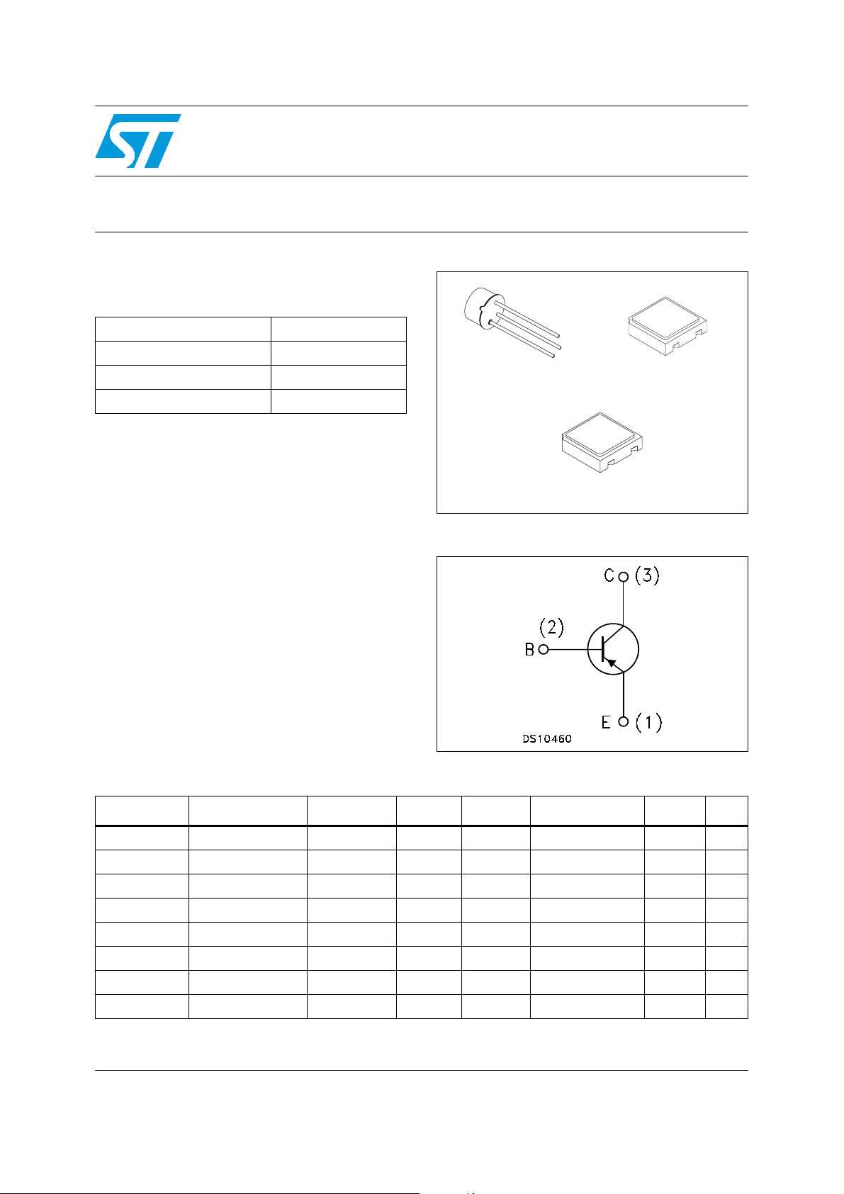
2N5401HR
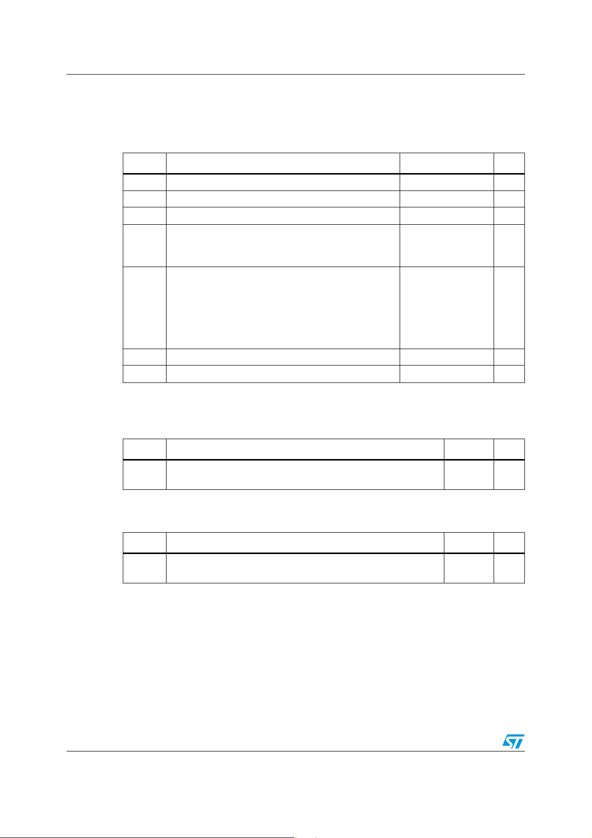
3
1
2
3
TO-18 LCC-3
3
1
2
■ Hi-Rel PNP bipolar transistor
■ Linear gain characteristics
■ ESCC qualified
■ European preferred part list - EPPL
■ 100 krad low dose rate
■ Radiation level: lot specific total dose contact
Figure 1. Internal schematic diagram
4
1
2
LCC-3UB
marketing for specified level
Description
The 2N5401HR is a silicon planar epitaxial PNP
transistor in TO-18 and LCC-3 packages. It is
specifically designed for aerospace Hi-Rel
applications and ESCC qualified according to the
5202-014 specification. In case of conflict
between this datasheet and ESCC detailed
specification, the latter prevails.
Table 1. Device summary
Order codes ESCC Part num. Quality Level Rad level Packages Lead Finish Mass (g) EPPL
2N5401UB1 - Eng. Model LCC-3UB Gold 0.06 -
SOC5401SW 5202/014/07 ESCC Flight 100 krad LCC-3 Solder Dip 0.06 Y
2N5401UB06 5202/014/06 ESCC Flight LCC-3UB Gold 0.06 -
2N5401UB07 5202/014/07 ESCC Flight LCC-3UB Solder Dip 0.06 -
SOC5401 - Eng. Model LCC-3 Gold 0.06 -
SOC5401HRB 5202/014/04 or 05 ESCC Flight LCC-3 Gold/Solder Dip
(1)
0.06 Y
2N5401/T1 - Eng. Model TO-18 Gold 0.40 -
2N5401HR 5202/014/01 or 02 ESCC Flight TO-18 Gold/Solder Dip
1. Depending ESCC part number mentioned on the purchase order.
(1)
0.40 -
July 2010 Doc ID 16934 Rev 2 1/10
www.st.com
10
Electrical ratings 2N5401HR
1 Electrical ratings
Table 2. Absolute maximum ratings
Symbol Parameter Value Unit
V
V
V
Collector-base voltage (IE = 0) -160 V
CBO
Collector-emitter voltage (IB = 0) -150 V
CEO
Emitter-base voltage (IC = 0) -5 V
EBO
Collector current
I
for 2N5401HR
C
for SOC5401HRB
Total dissipation at T
amb
≤ 25 °C
for 2N5401HR
P
for SOC5401HRB
TOT
for SOC5401HRB
(1)
-0.6
-0.5
0.36
0.36
0.58
Total dissipation at Tc ≤ 25 °C
for 2N5401HR
T
1. When mounted on a 8x10x0.6 mm ceramic substrate.
Storage temperature -65 to 200 °C
STG
T
Max. operating junction temperature 200 °C
J
1.2
Table 3. Thermal data for through-hole package
Symbol Parameter Value Unit
R
R
Thermal resistance junction-case __ max
thJC
Thermal resistance junction-ambient __ max
thJA
146
486
°C/W
°C/W
A
A
W
W
W
W
Table 4. Thermal data for SMD package
Symbol Parameter Value Unit
R
1. When mounted on a 8x10x0.6 mm ceramic substrate.
2/10 Doc ID 16934 Rev 2
Thermal resistance junction-ambient __ max
thJA
Thermal resistance junction-ambient
(1)
__ max
486
302
°C/W
°C/W

2N5401HR Electrical characteristics
2 Electrical characteristics
T
= 25 °C unless otherwise specified.
case
Table 5. Electrical characteristics
Symbol Parameter Test conditions Min. Typ. Max. Unit
I
CBO
I
EBO
V
(BR)CBO
V
(BR)CEO
V
(BR)EBO
V
CE(sat)
V
BE(sat)
h
FE
Collector-base cut-off
current (I
= 0)
E
Emitter-base cut-off
current (I
= 0)
C
= -120 V
V
CB
V
= -120 V TC = 150 °C
CB
= -3 V -50 nA
V
EB
-50
-50nAµA
Collector-base
breakdown voltage
= 0)
(I
E
= -100 µA -160 V
I
C
Collector-emitter
(1)
breakdown voltage
(I
= 0)
B
= -1 mA -150 V
I
C
Emitter-base
breakdown voltage
= 0)
(I
C
Collector-emitter
(1)
saturation voltage
Base-emitter
(1)
saturation voltage
(1)
DC current gain
h
fe
Small signal current
gain
= -10 µA -5 V
I
E
= -10 mA IB = -1 mA
I
C
IC = -50 mA IB = -5 mA
= -10 mA IB = -1 mA
I
C
IC = -50 mA IB = -5 mA
= -1 mA V
I
C
IC = -10 mA V
I
= -50 mA V
C
IC = -10 mA V
T
= -55 °C
amb
= -10 V IC = -10 mA
V
CE
CE
CE
CE
CE
= -5 V
= -5 V
= -5 V
= -5 V
f = 10 kHz
50
60
60
20
5
-0.2
-0.5
-1
-1
240
V
V
V
V
C
obo
1. Pulsed duration = 300 µs, duty cycle ≤ 2 %
Output capacitance
(I
= 0)
E
V
Doc ID 16934 Rev 2 3/10
= -10 V f = 1 MHz 6 pF
CB
 Loading...