

Hi-Rel NPN bipolar transistor 80 V - 5 A
Features
BV
CEO
(max) 5 A
I
C
H
at 10 V - 150 mA > 70
FE
Operating temperature range - 65 °C to + 200 °C
■ Hi-Rel NPN bipolar transistor
■ Linear gain characteristics
■ ESCC qualified
■ European preferred part list - EPPL
■ Radiation level: lot specific total dose contact
marketing for specified level
80 V
2N5154HR
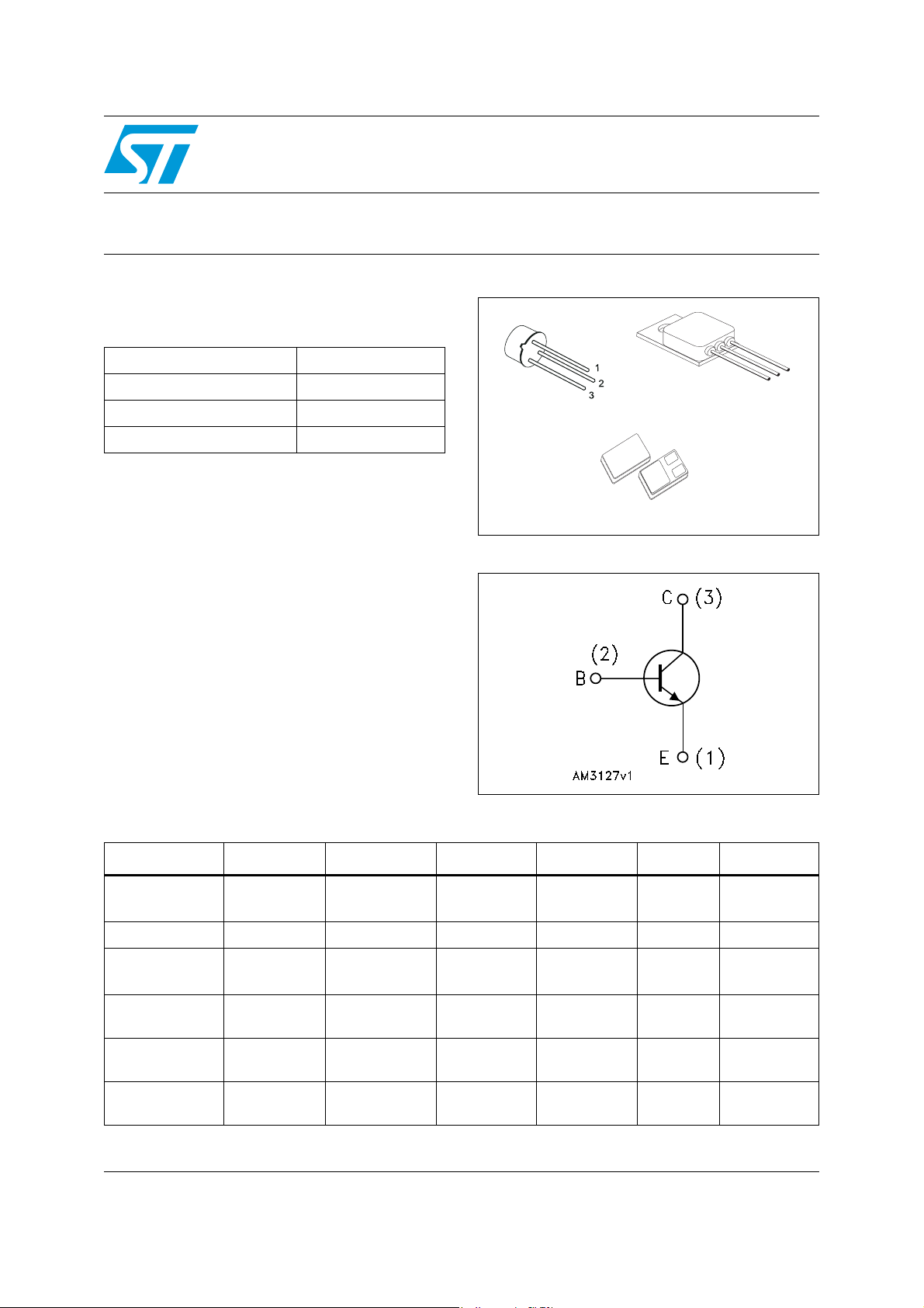
TO-39
SMD.5
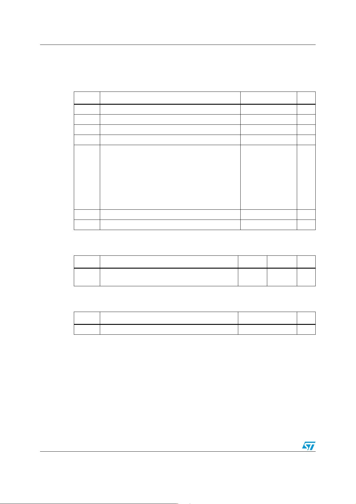
Figure 1. Internal schematic diagram
TO-257
2
1
3
1
3
2
Description
The 2N5154HR is a silicon planar epitaxial NPN
transistor in TO-39, TO-257 and SMD.5 packages.
It is specifically designed for aerospace Hi-Rel
applications and ESCC qualified according to the
5203-010 specification. In case of conflict
between this datasheet and ESCC detailed
specification, the latter prevails.
Table 1. Device summary
Order codes Packages Lead finish Marking Type EPPL Packaging
2N5154HR TO-39
Gold
Solder Dip
2N5154SHR SMD.5 Gold 520301006 ESCC Flight Yes Strip pack
2N5154ESYHRB TO-257
Gold
Solder Dip
2N5154T1 TO-39 Gold 2N5154T1
2N5154S1 SMD.5 Gold 2N5154S1
2N5154ESY TO-257 Gold 2N5154ESY
520301001
520301002
520301004
520301005
ESCC Flight Strip pack
ESCC Flight Strip pack
Engineering
model
Engineering
model
Engineering
model
Strip pack
Strip pack
Strip pack
July 2011 Doc ID 15387 Rev 3 1/10
www.st.com
10
Electrical ratings 2N5154HR
1 Electrical ratings
Table 2. Absolute maximum ratings
Symbol Parameter Value Unit
V
V
V
P
T
Collector-base voltage (IE = 0) 100 V
CBO
Collector-emitter voltage (IB = 0) 80 V
CEO
Emitter-base voltage (IC = 0) 6 V
EBO
I
Collector current 5 A
C
Total dissipation at T
for 2N5154HR
for 2N5154ESYHRB
for 2N5154SHR
TOT
T
for 2N5154HR
for 2N5154ESYHRB
for 2N5154SHR
Storage temperature - 65 to 200 °C
STG
T
Max. operating junction temperature 200 °C
J
amb
≤ 25 °C
C
≤ 25 °C
1
3.3
3.3
8.75
35
35
Table 3. Thermal data for through-hole packages
Symbol Parameter TO-39 TO-257 Unit
R
R
Thermal resistance junction-case __ max
thJC
Thermal resistance junction-ambient __ max
thJA
20
175
53
5
°C/W
W
W
W
W
W
W
Table 4. Thermal data for SMD package
Symbol Parameter SMD.5 Unit
R
2/10 Doc ID 15387 Rev 3
Thermal resistance junction-case __ max 5 °C/W
thJC
2N5154HR Electrical characteristics
2 Electrical characteristics
T
= 25 °C unless otherwise specified
case
Table 5. Electrical characteristics
Symbol Parameter Test conditions Min. Typ. Max. Unit
I
CES
I
EBO
I
CEO
V
(BR)CEO
V
CE(sat)
V
BE(sat)
h
FE
C
h
fe
OBO
Collector cut-off
current (I
Emitter cut-off current
= 0)
(I
C
Collector cut-off
current (IB = 0)
Collector-emitter
(1)
breakdown voltage
= 0)
(I
B
Collector-emitter
(1)
saturation voltage
Base-emitter
(1)
saturation voltage
(1)
DC current gain
AC forward current
transfer ratio
Output capacitance
= 0)
E
= 60 V
V
CB
V
= 60 V T
CB
= 5 V
V
EB
V
= 6 V
EB
= 40 V 50 µA
V
CE
= 150 °C
amb
10
1
µA
µA
1
µA
1
mA
IC = 100 mA 80 V
= 5 A IB = 0.5 A
I
C
IC = 2.5 A IB = 250 mA
= 2.5 A IB = 0.25 A
I
C
IC = 5 A IB = 0.5 A
I
= 50 mA V
C
IC = 2.5 A V
= 5 A V
I
C
= 2.5 A V
I
C
T
= - 55 °C
amb
= 5 V IC = 500 mA
V
CE
CE
CE
CE
CE
= 5 V
= 5 V
= 5 V
= 5 V
f = 20 MHz
IE = 0 V
CB
= 10 V
f = 1 MHz
50
70
40
35
3.5
1.5
1.45VV
1.45
2.2
200
250 pF
V
V
V
t
on
Turn-on time
V
I
V
t
off
Turn-off time
V
I
1. Pulsed duration = 300 µs, duty cycle ≤ 2%
Doc ID 15387 Rev 3 3/10
= 30 V V
CC
≅ 51 V I
in
= - I
B1
CC
in
B1
= 0.5 A
B2
= 30 V V
≅ 51 V I
= - I
= 0.5 A
B2
BB
C
BB
C
= 4 V
= 5 A
= 4 V
= 5 A
0.5 µs
1.3 µs
 Loading...