

Hi-Rel PNP dual matched bipolar transistor 60 V - 0.05 A
1
2
3
4
5
6
Features
BV
CEO
(max) 0.05 A
I
C
H
at 10 V - 150 mA > 150
FE
Operating temperature range -65°C to +200°C
60 V
2N3810HR
■ Hi-Rel PNP dual matched bipolar transistor
■ Linear gain characteristics
■ ESCC qualified
■ European preferred part list - EPPL
■ Radiation level: lot specific total dose contact
marketing for specified level
Description
The 2N3810HR is a silicon planar epitaxial PNP
transistor in TO-78 and LCC-6 packages. It is
specifically designed for aerospace Hi-Rel
applications and ESCC qualified according to the
5207-005 specification. In case of conflict
between this datasheet and ESCC detailed
specification, the latter prevails.
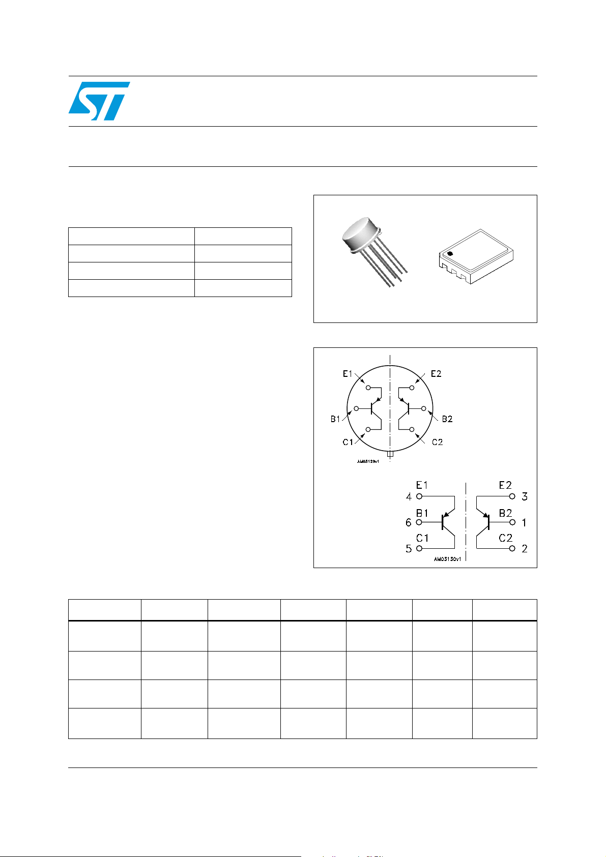
Table 1. Device summary
TO-78
LCC-6
Figure 1. Internal schematic diagram
for TO-78
for LCC-6
Order codes Packages Lead finish Marking Type EPPL Packaging
2N3810HR TO-78
Gold
Solder Dip
2N3810T1 TO-78 Gold 2N3810T1
SOC3810 LCC-6 Gold SOC3810
SOC3810HRB LCC-6
Gold
Solder Dip
520700501
520700502
520700507
520700509
ESCC Flight Strip pack
Engineering
model
Engineering
model
Strip pack
Waffle pack
ESCC Flight Yes Waffle pack
January 2010 Doc ID 15385 Rev 2 1/9
www.st.com
9

Electrical ratings 2N3810HR
1 Electrical ratings
Table 2. Absolute maximum ratings
Symbol Parameter Value Unit
V
V
V
P
Collector-base voltage (IE = 0) -60 V
CBO
Collector-emitter voltage (IB = 0) -60 V
CEO
Emitter-base voltage (IC = 0) -5 V
EBO
I
Collector current -50 mA
C
Total dissipation at T
for 2N3810HR
for 2N3810HR
for SOC3810HRB
TOT
for SOC3810HRB
amb
≤ 25 °C
(1)
(2)
(1) (3)
(2) (3)
0.5
0.6
0.6
1.2
Total dissipation at Tc ≤ 25 °C
for 2N3810HR
for 2N3810HR
T
1. One section.
2. Both sections.
3. When mounted on a 15 x 15 x 0.6 mm ceramic substrate.
Table 3. Thermal data for through-hole package
Storage temperature -65 to 200 °C
STG
T
Max. operating junction temperature 200 °C
J
(1)
(2)
0.5
0.6
Symbol Parameter Value Unit
R
Thermal resistance junction-case
thJC
Thermal resistance junction-case
R
Thermal resistance junction-ambient
thJA
Thermal resistance junction-ambient
1. One section.
2. Both sections.
(1)
__ max
(2)
__ max
(1)
__ max
(2)
__ max
350
292
350
292
°C/W
°C/W
°C/W
°C/W
W
W
W
W
W
W
Table 4. Thermal data for SMD package
Symbol Parameter Value Unit
R
1. One section.
2. Both sections.
3. When mounted on a 15 x 15 x 0.6 mm ceramic substrate.
Thermal resistance junction-ambient
thJA
Thermal resistance junction-ambient
(1)(3)
(2)(3)
2/9 Doc ID 15385 Rev 2
__ max
__ max
292
146
°C/W
°C/W

2N3810HR Electrical characteristics
2 Electrical characteristics
T
= 25 °C unless otherwise specified.
case
Table 5. Electrical characteristics
Symbol Parameter Test conditions Min. Typ. Max. Unit
V
V
(BR)CEO
V
V
CE(sat)
V
BE(sat)
h
FE2-1
I
CBO
I
EBO
(BR)CBO
(BR)EBO
(1)
h
FE
/ h
FE2-2
Collector-base cut-off
current (I
Emitter-base cut-off
current (IC = 0)
Collector-base
breakdown voltage
= 0)
(I
E
Collector-emitter
(1)
breakdown voltage
= 0)
(I
B
Emitter-base
breakdown voltage
(IC = 0)
Collector-emitter
(1)
saturation voltage
Base-emitter
(1)
saturation voltage
DC current gain
DC current ratio
comparison
= 0)
E
= -50 V
V
CB
V
= -50 V TC = 150 °C
CB
= -4 V -20 nA
V
EB
-10
-10nAµA
IC = -10 µA -60 V
IC = -10 mA -60 V
IE = -10 µA -5 V
= -100 µA IB = -10 µA
I
C
IC = -1 mA IB = -100 µA
= -100 µA IB = -10 µA
I
C
IC = -1 mA IB = -100 µA
= -10 µA V
I
C
IC = -100 µA V
= -500 µA V
I
C
= -1 mA V
I
C
IC = -10 mA V
= -100 µA V
I
C
= -55 °C
T
amb
I
= -100 µA V
C
= -5 V
CE
= -5 V
CE
= -5 V
CE
= -5 V
CE
= -5 V
CE
= -5 V
CE
= -5 V 0.91 1.1
CE
100
150
150
150
125
60
-0.2
-0.25VV
-0.7
-0.8VV
450
450
450
h
FE2-1
Δ⏐V
Δ⏐V
= -100 µA V
/ h
BE1
V
BE2
BE1
V
BE2
DC current ratio
FE2-2
comparison
-
Base-emitter voltage
⏐
differential
-
Base-emitter voltage
⏐
differential
Leakage current
I
Lk
between active
devices
h
fe
Small signal current
gain
I
C
= -55 °C to +125 °C
T
amb
= -5 V IC = -10 µA
V
CE
V
= -5 V IC = -100 µA
CE
= -5 V IC = -10 mA
V
CE
= -5 V IC = -100 µA
V
CE
= -55 °C to +25 °C
T
amb
= +25 °C to +125 °C
T
amb
V = -50 V to E2, B2, C
V = 0 V to E1, B1, C
= -5 V IC = -10 mA
V
CE
f = 1 kHz
CE
= -5 V
2
1
0.85 1.18
5
3
5
0.81mV
-5 µA
125
mV
mV
mV
mV
Doc ID 15385 Rev 2 3/9
 Loading...