


Hi-Rel NPN bipolar transistor 60 V - 50 mA
Features
Parameter Value
BV
CEO
(max) 50 mA
I
C
h
at 10 V - 150 mA > 250
FE
Operating temperature range - 65 °C to + 200 °C
■ Linear gain characteristics
■ Hermetic packages
■ ESCC qualified
■ European preferred part list - EPPL
60 V
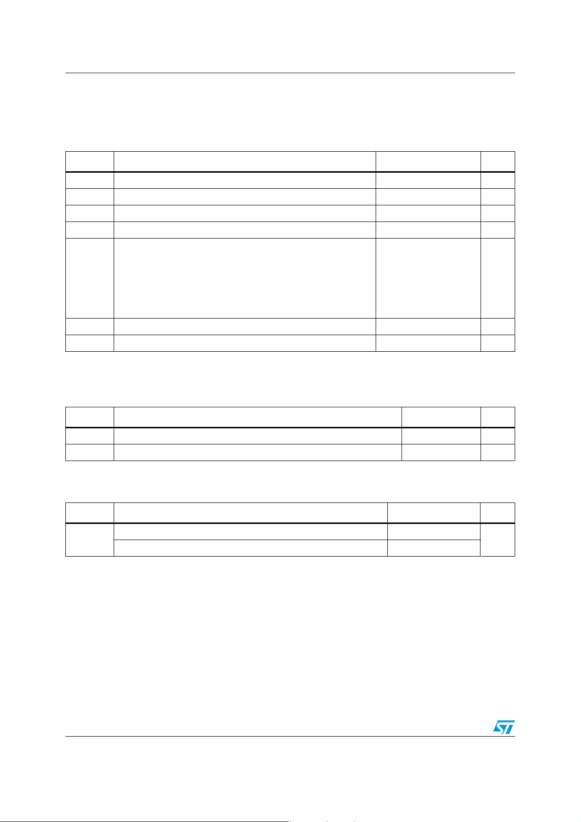
2N2484HR
1
2
3
TO-18
3
1
2
LCC-3
Figure 1. Internal schematic diagram
3
4
2
LCC-3UB
1
Description
The 2N2484HR is a silicon planar epitaxial NPN
transistor specifically designed for aerospace HiRel applications and housed in hermetic
packages. It complies with the ESCC 5000
qualification standard. It is ESCC qualified
according to the 5201-001 specification. In case
of conflict between this datasheet and ESCC
detailed specification, the latter prevails.
Pin 4 in LCC-3UB connected to the lid (for ground contact)
Table 1. Device summary
Order codes ESCC Part number Quality Level Packages Lead Finish Mass (g) EPPL
2N2484UB1 -
2N2484UB06 5201/001/06 ESCC Flight LCC-3UB Gold 0.06 -
2N2484UB07 5201/001/07 ESCC Flight LCC-3UB Solder Dip 0.06 -
SOC2484 -
SOC2484HRB 5201/001/01 or 02 ESCC Flight LCC-3 Gold / Solder Dip
2N2484HR 5201/001/04 or 05 ESCC Flight TO-18 Gold / Solder Dip
1. Depending ESCC part number mentioned on the purchase order.
Engineering
Model
Engineering
Model
LCC-3UB Gold 0.06 -
LCC-3 Gold 0.06 -
(1)
(1)
0.06 -
0.40 Y
July 2010 Doc ID 17734 Rev 1 1/12
www.st.com
12
Electrical ratings 2N2484HR
1 Electrical ratings
Table 2. Absolute maximum ratings
Symbol Parameter Value Unit
V
V
V
P
CBO
CEO
EBO
I
TOT
Collector-base voltage (IE = 0) 60 V
Collector-emitter voltage (IB = 0) 60 V
Emitter-base voltage (IC = 0) 6 V
Collector current 50 mA
C
Total dissipation at T
2N2484HR
2N2484UB1 / SOC2484HRB
2N2484UB1 / SOC2484HRB
amb
≤ 25 °C
(1)
0.36
0.36
0.73
Total dissipation at Tc ≤ 25 °C
for 2N2484HR
T
STG
T
1. When mounted on a 15 x 15 x 0.6 mm ceramic substrate.
Storage temperature - 65 to 200 °C
Max. operating junction temperature 200 °C
J
1.2
Table 3. Thermal data for through-hole package
Symbol Parameter TO-18 Unit
R
R
thJC
thJA
Thermal resistance junction-case __ max 146 °C/W
Thermal resistance junction-ambient __ max 486 °C/W
W
W
W
W
Table 4. Thermal data for SMD package
Symbol Parameter LCC-3 / LCC-3UB Unit
R
thJA
1. When mounted on a 15 x 15 x 0.6 mm ceramic substrate.
2/12 Doc ID 17734 Rev 1
Thermal resistance junction-ambient __ max 486
(1)
Thermal resistance junction-ambient
max 239
°C/W
2N2484HR Electrical characteristics
2 Electrical characteristics
T
= 25 °C unless otherwise specified.
case
Table 5. Electrical characteristics
Symbol Parameter Test conditions
(1)
Min. Typ. Max. Unit
V
(BR)CBO
V
(BR)CEO
V
(BR)EBO
I
CBO
I
CBO
V
CE(SAT)
h
FE
(2)
Collector-base
breakdown voltage
Collector-emitter
(2)
breakdown voltage
Emitter-base breakdown
voltage
Collector-base cut-off
current
Emitter-base cut-off
current
Collector-emitter
(2)
saturation voltage
DC forward current
transfer ratio
High frequency current
Gain 1
h
fe
High frequency current
Gain 2
C
obo
C
ibo
h
FE
h
ie
h
oc
h
re
N
FW
Output capacitance
Input capacitance
Small signal current gain
Small signal input
impedance
Small signal output
impedance
Small signal reverse
voltage transfer ratio
Wide-Band noise
I
= 10 µA 60 - V
C
= 10 mA 60 - V
I
C
= 10 µA 6 - V
I
E
V
= 45 V - 10 nA
CB
V
= 5 V - 10 nA
EB
= 1 mA IB = 0.1 mA - 0.35 V
I
C
IC = 1 µA V
= 10 µA V
I
C
= 100 µA V
I
C
IC = 1 mA V
= 10 mA V
I
C
= 5 V IC = 50 µA
V
CE
f = 5 MHz
= 5 V IC = 500 µA
V
CE
f = 30 MHz
V
= 5 V IE = 0
CB
f = 1 MHz
V
= 0.5 V IC = 0
EB
f = 1 MHz
I
= 1 mA V
C
f = 1 kHz
= 1 mA V
I
C
f = 1 kHz
= 1 mA V
I
C
f = 1 kHz
= 1 mA V
I
C
f = 1 kHz
V
= 5 V IC = 10 µA
CE
= 10 kΩ
R
S
CE
CE
CE
CE
CE
CE
CE
CE
CE
= 5 V
= 5 V
= 5 V
= 5 V
= 5 V
= 5 V
= 5 V
= 5 V
= 5 V
30
100
175
250
500
-
550
650
800
3-
2-
-6pF
-6pF
150 - 900
3.5 - 24 kΩ
-40µmho
- 800 10
-3dB
-6
Doc ID 17734 Rev 1 3/12
Electrical characteristics 2N2484HR
Table 5. Electrical characteristics
Symbol Parameter Test conditions
V
= 5 V IC = 10 µA
CE
NF
N1
= 10 kΩ f = 100 Hz
R
S
Power BW = 200 Hz
V
= 5 V IC = 10 µA
CE
N2
Spot noise figure
= 10 kΩ f = 1 kHz
R
S
Power BW = 20 Hz
V
= 5 V IC = 10 µA
CE
NF
N3
RS = 10 kΩ f = 10 kHz
Power BW = 2 Hz
1. Measurement performed on a sample basis, LTPD 7 or less.
2. Pulse measurement: Pulse width ≤ 300 µs, duty cycle ≤ 1.0 %
(1)
Min. Typ. Max. Unit
-3
-10
dBNF
-2
Table 6. Electrical characteristics at high and low temperatures
Symbol Parameter Test conditions Min. Typ. Max. Unit
I
CBO
h
FE2
Collector-base cut-off
current
DC forward current
transfer ratio
V
= 45 V T
CB
= 10 µA V
I
C
T
= - 55 °C
amb
= 150 °C - 10 µA
amb
= 5 V
CE
20 -
4/12 Doc ID 17734 Rev 1
 Loading...