

Features
1N6642U
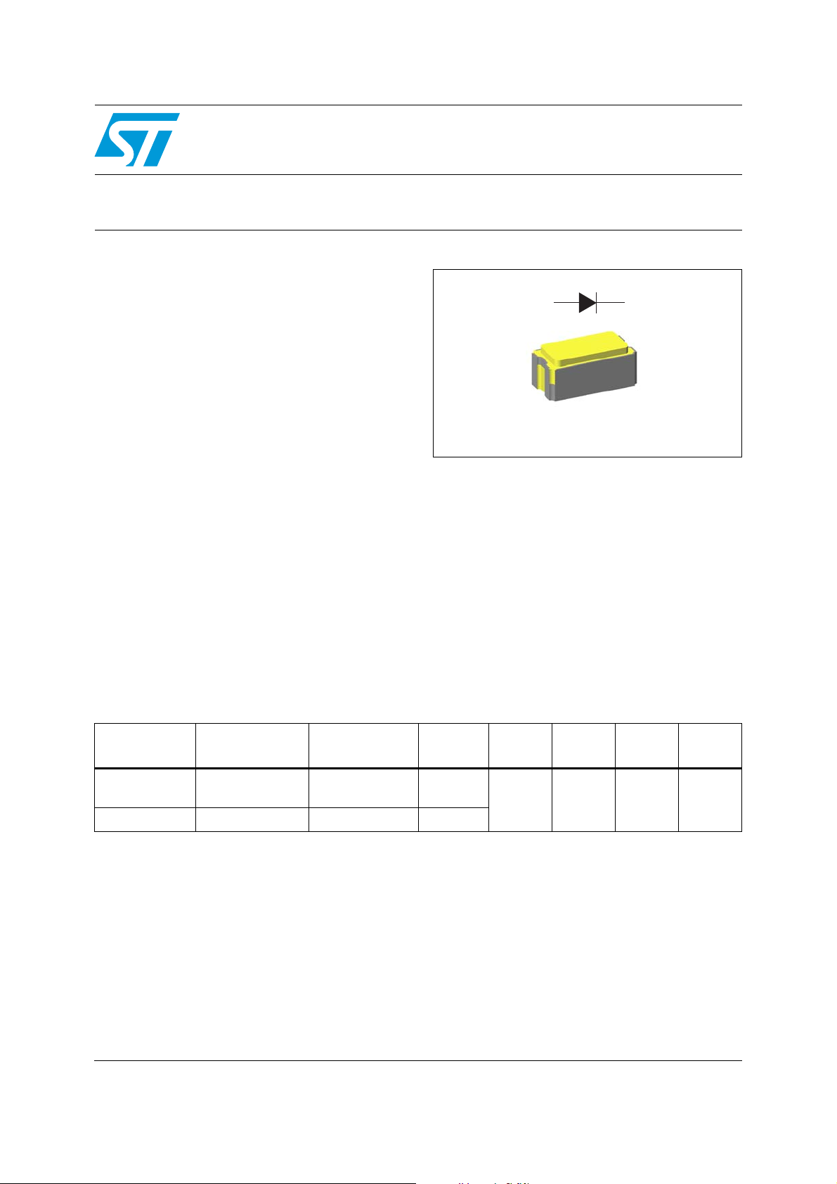
Aerospace 0.3 A - 100 V switching diode
■ Surface mount hermetic package
■ High thermal conductivity materials
■ Very small conduction losses
■ Negligible switching losses
■ Extremely fast switching
■ Low forward voltage drop
■ Target radiation qualification:
– 150 krad (Si) low dose rate
– 3 Mrad high dose rate
■ Package weight: 0.12 g
Table 1. Device summary
(1)
A
K
K
A
LCC-2D
Description
This power ultrafast recovery rectifier is designed
and packaged to comply with the ESCC5000
specification for aerospace products. It is housed
in a surface mount hermetically sealed LCC-2D
package whose footprint is 100% compatible with
industry standard solutions in D5A.
The 1N6642U is suitable for switching mode
power supplies and high frequency DC to DC
converters such as low voltage high frequency
inverter, free wheeling or polarity protection.
Order code
1N6642UD1 -
1N6642U02D 5101/026/xx Flight part Target
1. Contact ST sales office for information about the specific conditions for products in die form and gold plated version.
September 2011 Doc ID 16972 Rev 2 1/7
ESCC detailed
specification
Quality level EPPL I
Engineering
model
-
V
F(AV)
0.3 A 100 V 175 °C 1.2 V
RRM
T
j(max)
V
F (max)
www.st.com
7
Characteristics 1N6642U
1 Characteristics
Table 2. Absolute ratings (limiting values)
Symbol Parameter Value Unit
V
RRM
I
F(RMS)
I
F(AV)
I
FSM
T
stg
T
T
sol
1. For all variants at Tc ≥ +155 °C per diode, derate linearly to 0 A at +175 °C.
2. Maximum duration 5 s. The same package must not be re-soldered until 3 minutes have elapsed.
Repetitive peak reverse voltage 100 V
Forward rms current 0.5 A
Average forward rectified current
Forward surge current
Storage temperature range -65 to +175 °C
Operating junction temperature range -65 to +175 °C
j
Maximum soldering temperature
(1)
(2)
t
= 8.3 ms sinusoidal,
p
≤ 25 °C
t
amb
300 mA
2A
245 °C
Table 3. Thermal resistance
Symbol Parameter Value Unit
Junction to case
R
th (j-c)
R
Junction to ambient 280
th (j-a)
1. Package mounted on infinite heatsink
Table 4. Static electrical characteristics
Symbol Parameter Tests conditions Min. Typ. Max. Unit
(1)
Breakdown voltage T
V
BR
(1)
I
R
V
F
1. Pulse test: tp = 10 ms, δ < 2%
2. Pulse test: tp = 680 µs, δ < 2%
Reverse current
(2)
Forward voltage
(1)
60
= 25 °C IR = 100 µA 100 - - V
j
°C/W
Tj = 25 °C VR = 20 V - - 25 nA
= 25 °C VR = 75 V - - 50 nA
T
j
= 150 °C VR = 20 V - - 30 µA
T
j
= 150 °C VR = 75 V - - 40 µA
T
j
Tj = 25 °C IF = 10 mA - - 800
= 25 °C IF = 100 mA - - 1200
T
j
= 150 °C IF = 10 mA - - 800
T
j
= -55 °C IF = 100 mA - - 1200
T
j
mV
To evaluate the conduction losses use the following equation:
P = 0.74 x I
2/7 Doc ID 16972 Rev 2
F(AV)
+ 1.00 x I
F2(RMS )
1N6642U Characteristics
Table 5. Dynamic characteristics
Symbol Parameter
IF = IR = 10 mA
t
V
t
FR
C
1. Guaranteed but not tested
Reverse recovery time
rr
Forward recovery voltage IFM = 200 mA - - 5 V
FP
= 1 A, Vr = 30 V, dI/dt = -15 A/µs 20
I
F
Forward recovery time IFM = 200 mA - - 20 ns
V
= 0 V, V = 50 mV, F = 1 MHz - - 5 pF
Diode capacitance
j
R
= 1.5 V, V = 50 mV, F = 1 MHz - - 2.8 pF
V
R
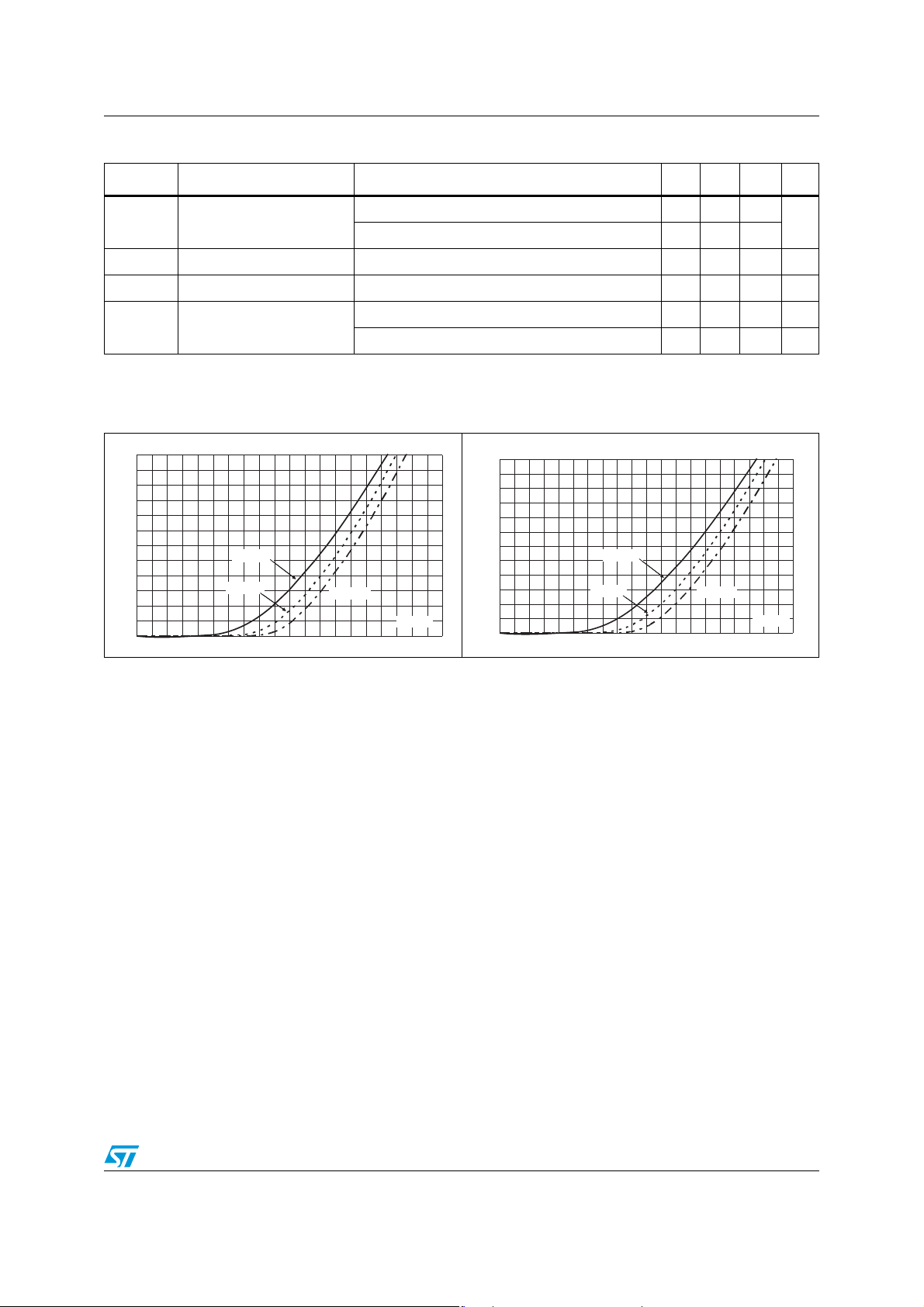
Figure 1. Forward voltage drop versus
forward current (typical values)
I (A)
FM
1.2
1.0
0.8
0.6
0.4
0.2
0.0
0.0 0.2 0.4 0.6 0.8 1.0 1.2 1.4 1.6 1.8 2.0
Tj=150 °CTj=150 °C
Tj=25 °CTj=25 °C
Tj=-55 °C
V (V)
FM
Test conditions
(1)
Min. Typ. Max. Unit
--9
Figure 2. Forward voltage drop versus
forward current (maximum values)
I (A)
FM
1.2
1.0
0.8
0.6
0.4
0.2
0.0
0.0 0.2 0.4 0.6 0.8 1.0 1.2 1.4 1.6 1.8 2.0
Tj=150 °CTj=150 °C
Tj=25 °CTj=25 °C
Tj=-55 °C
V (V)
FM
ns
Doc ID 16972 Rev 2 3/7
 Loading...