

Page 1

A TI REF
5050
220
220
.1 uF
332J100
20.000
TL074CN
TL074CN
TL074CN
CD4011BE
CD40106BE
TL072P
TL072P
TL072P
LM393P
LF
442CN
SSSR Labs MCU Chip
KOTELNIKOV 1.2
CD4042BE
KP590KH5
AD7545A
SM042, Assembly Manual
PCB Version 1.2
Page 2

SM042, Assembly Manual
PCB Version 1.2
Step 1: PCB Top Side
The SM042 DIY Kit contains two boards:
Circuit board 1. (Rear) This board consists of the main powering, VCO and TG circuitry.
Circuit board 2. (Front) This board contains interface circuitry and the linear scaling
circuitry for CV and reference voltage.
Most of the components have to be placed on the top side of both boards, but pinheader connectors and couple of aluminium capacitors are have to be soldered to the
bottom side
The order of assembly briefly can be described like that: Install SMD components,
small diodes, horizontally placed resistors, IC sockets, small capacitors, the rest of
non-mechanical components, then LED, pin-headers and bottom-side capacitors, then
install all chips, power and jumper connectors, the tactile switch, then toggle
switches, potentiometers and jack sockets. The following manual will guide you
through the assembling process in details.
Page 2 of 18
Page 3
A TI REF
5050
A TI REF
5050
SM042, Assembly Manual
PCB Version 1.2
Pin 1
Key dot
Order of soldering
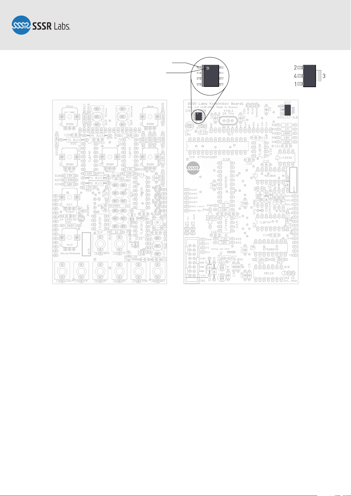
Step 2: SMD Components
The AMS1117-5.0 and REF5050 are the only two SMD components in our DIY kit. Place
the AMS1117 chip accurately aligned to its footprint, then solder pins according to the
order given in the picture above. The pin 4 (heatsink) will require long heating up. Don’t
worry about the overheating, this component is designed to be heated seriously! Install
the REF5050 chip oriented as shown on the picture above. Solder one of the pins in a
corner, align the chip well, solder the opposite corner, then the remaining pins.
Page 3 of 18
Page 4
A TI REF
5050
SM042, Assembly Manual
PCB Version 1.2
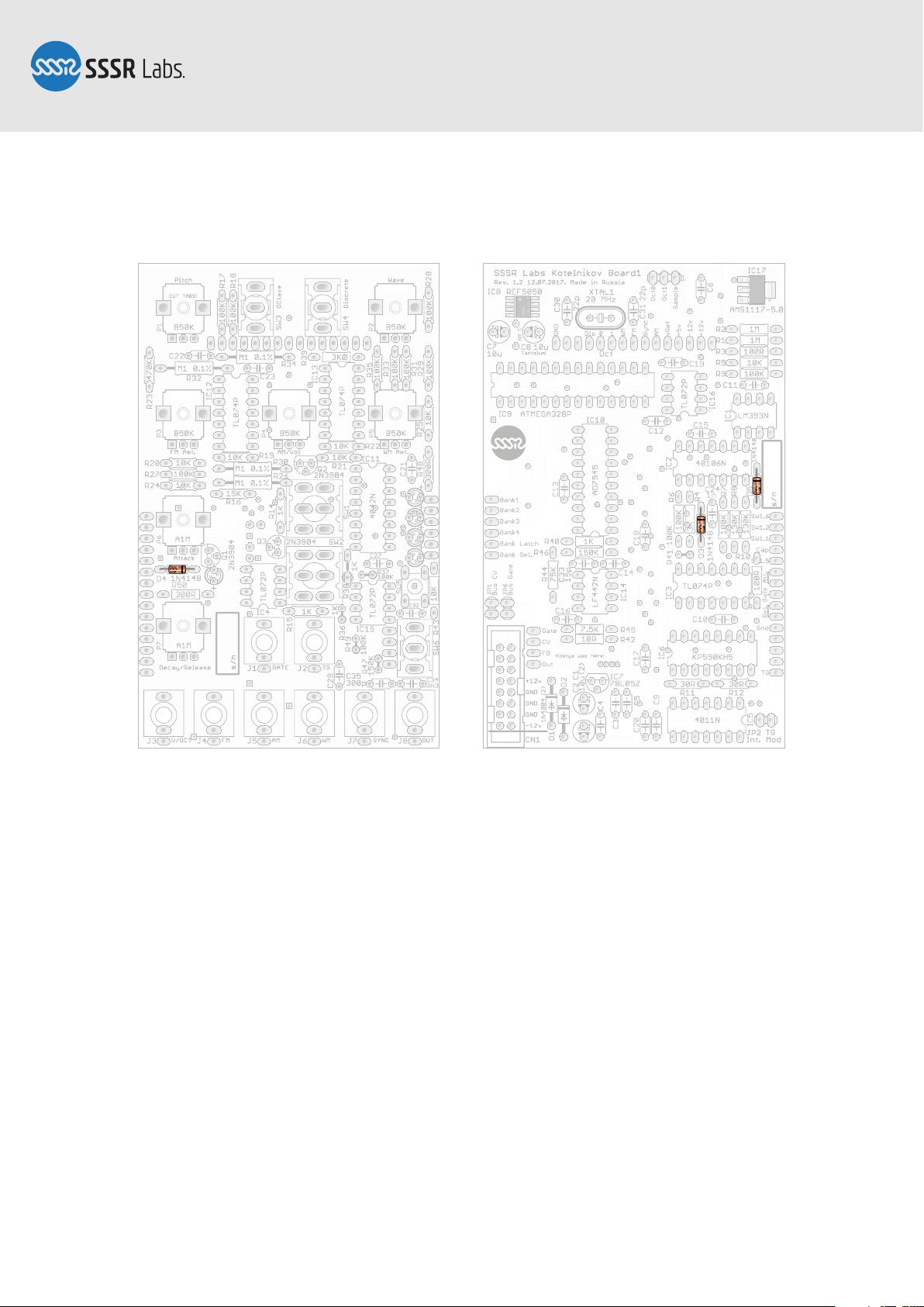
Step 3: Small Signal Diodes
Find the thinnest components: a silicon small-signal diodes. Notice the polarity. The
black stripes indicating the cathodes must correspond with stripes on the PCB. Solder
all diodes to the top side of the PCB, then proceed to step 4.
Page 4 of 18
Page 5
A TI REF
5050
Bend a bit
SM042, Assembly Manual
PCB Version 1.2
to the right
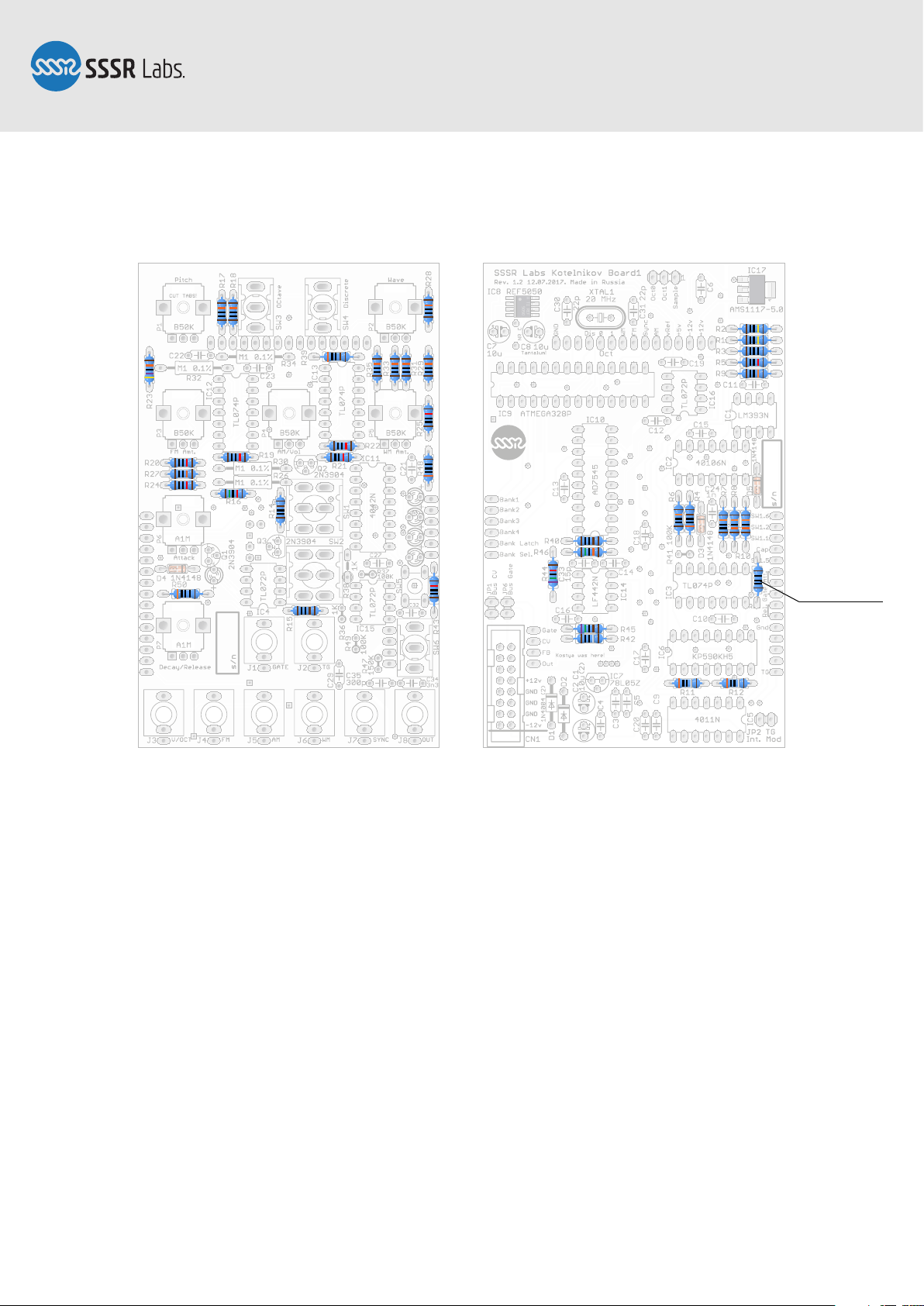
Step 4: Resistors
Install the resistors. You can use the above picture as the reference to verify values
before soldering.
Flip the PCB over, trim the pins and reflow and solder everything to the bottom side.
This technique is the best method to accurately and firmly solder axial components, so
it’s recommended to use it with all components allowing you access to the top side.
Page 5 of 18
Page 6
A TI REF
5050
Notch
SM042, Assembly Manual
PCB Version 1.2
Reverse direction!Pin 1
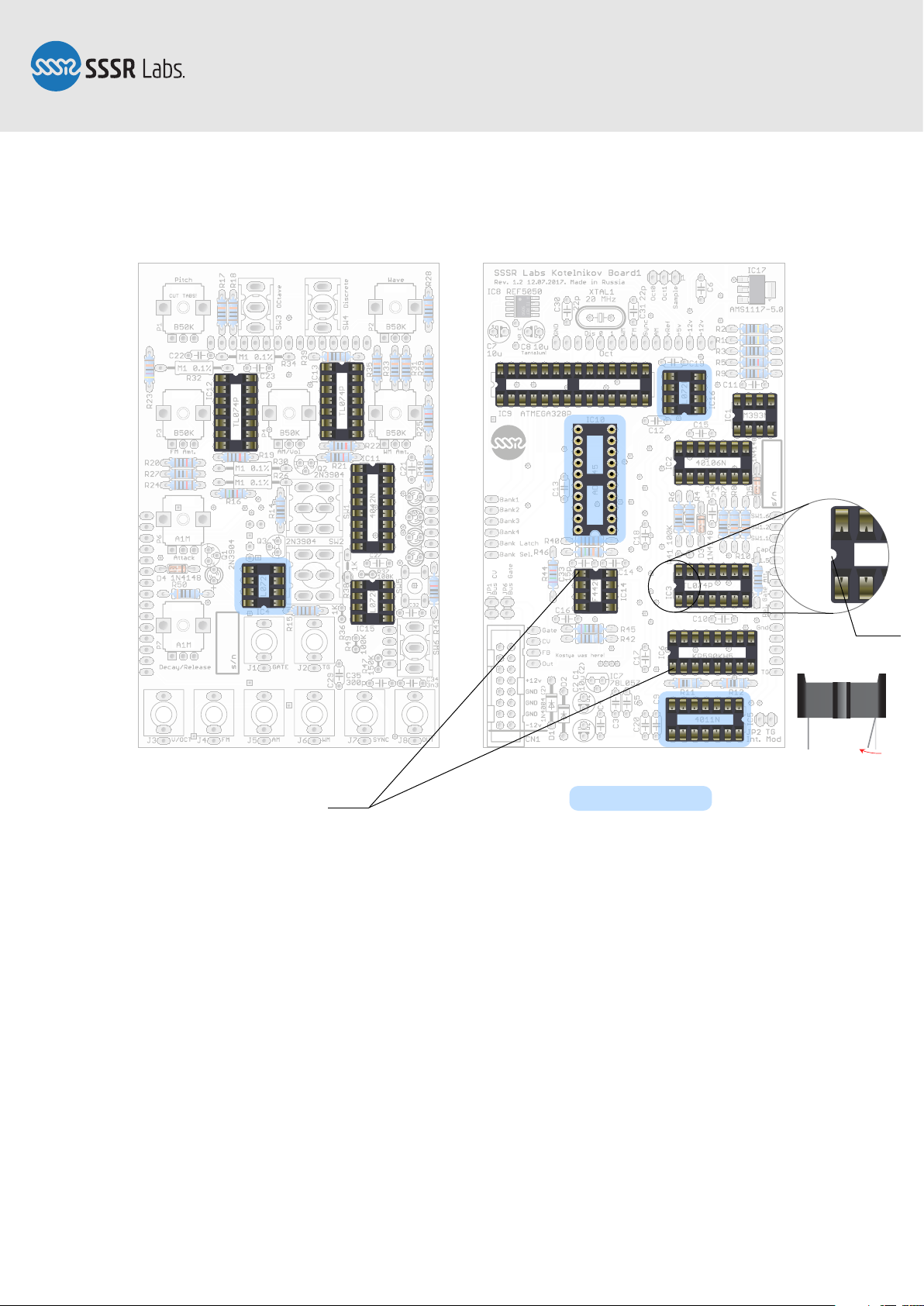
Step 5: IC Sockets
Insert all DIP IC sockets. Please pay double attention to the correct orientation. The
default orientation for chips in the module is the notch turned to the top, or to the left,
but there are chips with other directions, marked by blue areas in the picture.
These sockets are very slippy, so it’s practical to gently bend their pins towards each
other to help them fixate in the holes while you’re flipping the board over and soldering
them. It’s recommended to solder just two pins in the opposite corners of each socket
and then reflow them while pushing the socket closer to the surface of the PCB. Then
solder the remaining pins.
Page 6 of 18
Page 7
A TI REF
5050
SM042, Assembly Manual
PCB Version 1.2
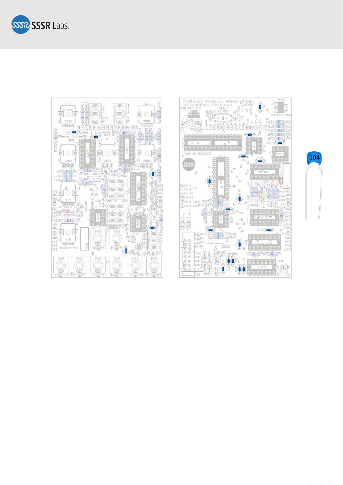
Step 6: Bypass Capacitors
Install and solder the 100 nF bypass capacitors, labelled as “104”. There are total of 21
of them. In some early kits, the MuRata ceramic capacitors was replaced with Epcos
polyester film capacitors.
Page 7 of 18
Page 8
A TI REF
5050
220
220
.1 uF
332J100
20.000
Identifying
SM042, Assembly Manual
PCB Version 1.2
capacitors:
22 or 220: 220 pF
.1μJ100
or μ10J100
or 104: 100 nF
331: 330 pF
(repl. for 300 pF)
15 or 150: 15 pF
1nJ100
or 102: 1 nF
332J100
or 332: 3.3 nF
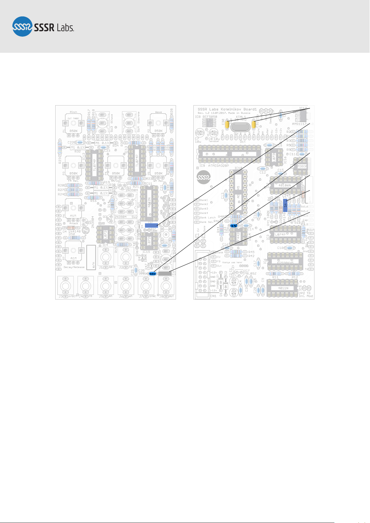
Step 7: Other Small Capacitors And Quartz Crystal
Install other small capacitors. You can identify them by labels listed on the picture.
Also, it's good to know that there are two types of notation for a capacitor value.
Style 1: 3-digit. The first two digits should be read as they are, and then you need to
add as much zeroes as are indicated by the third digit, and interpret this as the value in
pF. 150 means 15 pF, 334 means 330000 pF (= 330 nF). Very simple.
Style 2: The value usually consists of 2 or 3 digits and a letter p, n or u (µ) indicating
the unit of the value. This letter actually stands in place of the decimal point, so 33n
means 33 nF, 3n3 means 3.3 nF, and n33 means 0.33 nF (= 330 pF). The following
“J100” on film capacitors indicates the tolerance class, and the voltage rating.
Page 8 of 18
Page 9
A TI REF
5050
220
220
.1 uF
332J100
20.000
≤8 mm
SM042, Assembly Manual
PCB Version 1.2
≥3 mm
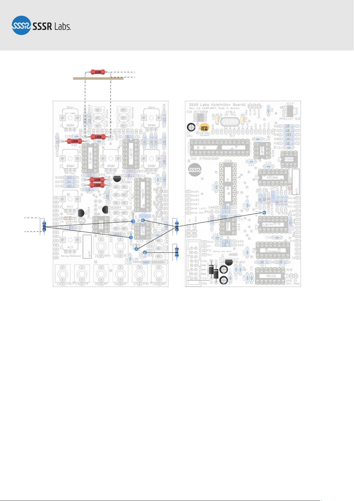
Step 8: Remaining Top-Side Components
Install precision 100K resistors into their places. They must be elevated above the
board as shown on the picture. This method of installation is required by the resistors'
design and it helps to keep values within tolerance. Then install rectifier diodes and
aluminium capacitors. All of those are all polarized components! As with the smallsignal diodes, cathodes of the rectifier diodes are marked with stripes on diodes and
footprints. All holes for the positive pins of electrolytic capacitors are marked with the
“+” sign. All positive pins on capacitors are longer than negative pins
Finally, install the vertically oriented resistors. The allowed height of the resistors
must be non greater than 8 mm to ensure that leads do not touch the surface of the
panel.
Page 9 of 18
Page 10
A TI REF
5050
220
220
.1 uF
332J100
20.000
SM042, Assembly Manual
PCB Version 1.2
Step 9: LED
Take two potentiometers or toggle switches, and two jack sockets. Install them into
places for P1, P2 (SW3, SW4), J1 and J2 but do not solder them. Then insert five LEDs
keeping the correct polarity. Anodes are indicated by the “+” sign on the board and the
longer pins. Remove the film from the front panel if there's any, and install the panel
onto the board through the switches and jack sockets. Holding the panel, turn the
module upside down and let all diodes slip into their holes. Then solder them one by
one keeping the correct clamping of the panel and LEDs' height.
Now, take off the panel and proceed to the next step.
Page 10 of 18
Page 11
3.3 μF 50v
SM042, Assembly Manual
PCB Version 1.2
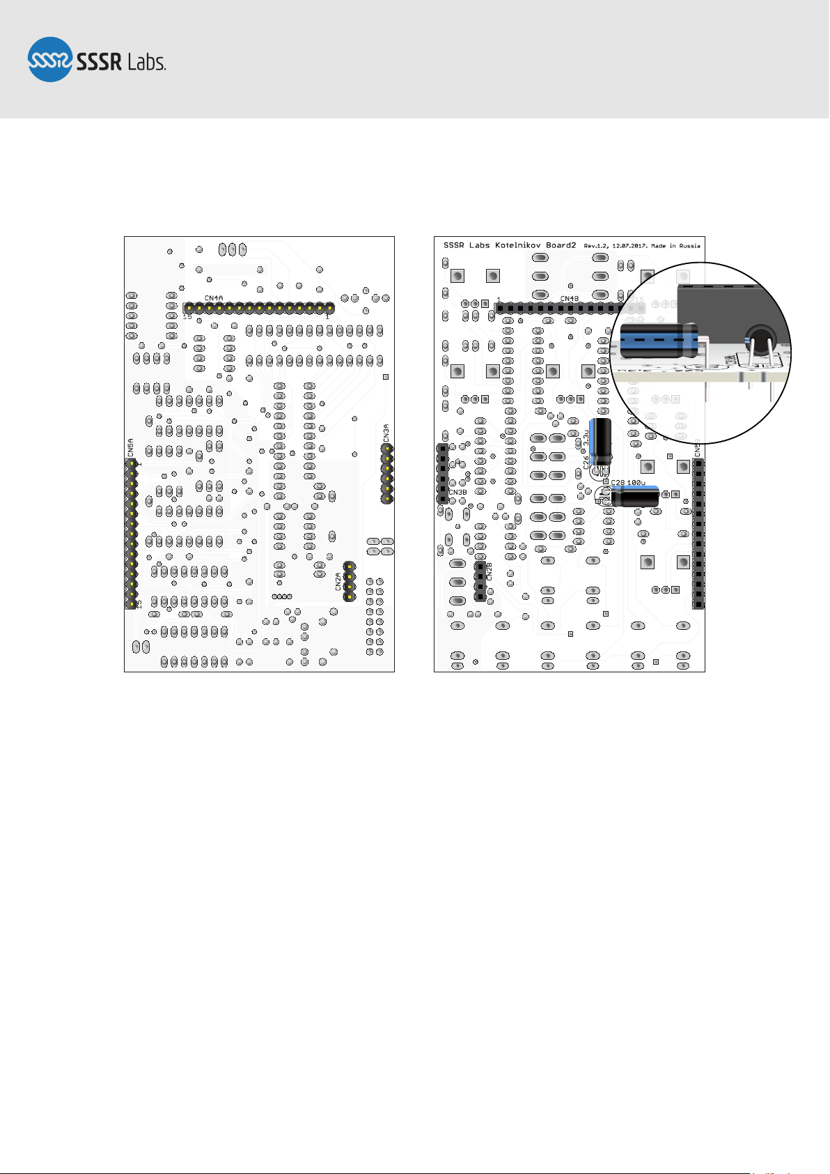
Step 10: Bottom Side Components
You will find 4 complementary pairs of pin-headers tied together: 2 × 15-pin, 1 × 4-pin
and 1 × 6-pin. The female part must be installed on Board 2, and the male part — on
Board 1. Install connectors on the bottom side of Board 1, then construct a sandwich
out of both boards as shown on the picture. Solder all headers ensuring that all construction is clamped tight and secure.
Insert electrolytic capacitors into the bottom side of Board 2. Bend them as shown on
the picture, and solder. The holes for the positive pins are indicated with white stripes
and the negative are black. The positive pins are longer than the negative.
Page 11 of 18
Page 12
A TI REF
5050
220
220
.1 uF
332J100
20.000
TL074CN
TL074CN
TL074CN
CD4011BE
CD40106BE
TL072P
TL072P
TL072P
LM393P
LF
442CN
SSSR Labs MCU Chip
KOTELNIKOV 1.2
CD4042BE
KP590KH5
AD7545A
SM042, Assembly Manual
PCB Version 1.2
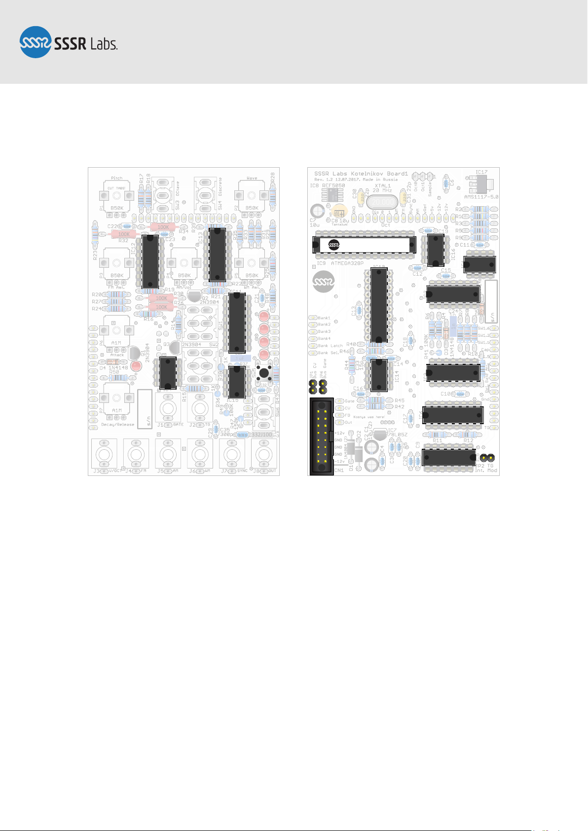
Step 11: Headers, Tactile Switch, IC
Install three 2-pin headers and wear the jumpers on. Then solder all headers.
Install the power pin-header. Notice the orientation! It’s recommended to solder two
pins in the opposite corners, then solder the remaining pins. The six pins from 3 to 8
are connected with the ground plane and require extra heating. It is also recommended to plug the power cable to prevent pins from bending if the plastic case has
started to melt due to extensive heating.
Insert all integrated circuits into their sockets. Refer to the picture for correct placement and orientation. Install and solder the tactile switch.
It’s highly recommended to clean the top sides of the boards now, before installing the
control hardware and the front panel.
Page 12 of 18
Page 13
A TI REF
5050
220
220
.1 uF
332J100
20.000
TL074CN
TL074CN
TL074CN
CD4011BE
CD40106BE
TL072P
TL072P
TL072P
LM393P
LF
442CN
SSSR Labs MCU Chip
KOTELNIKOV 1.2
CD4042BE
KP590KH5
AD7545A
SM042, Assembly Manual
PCB Version 1.2
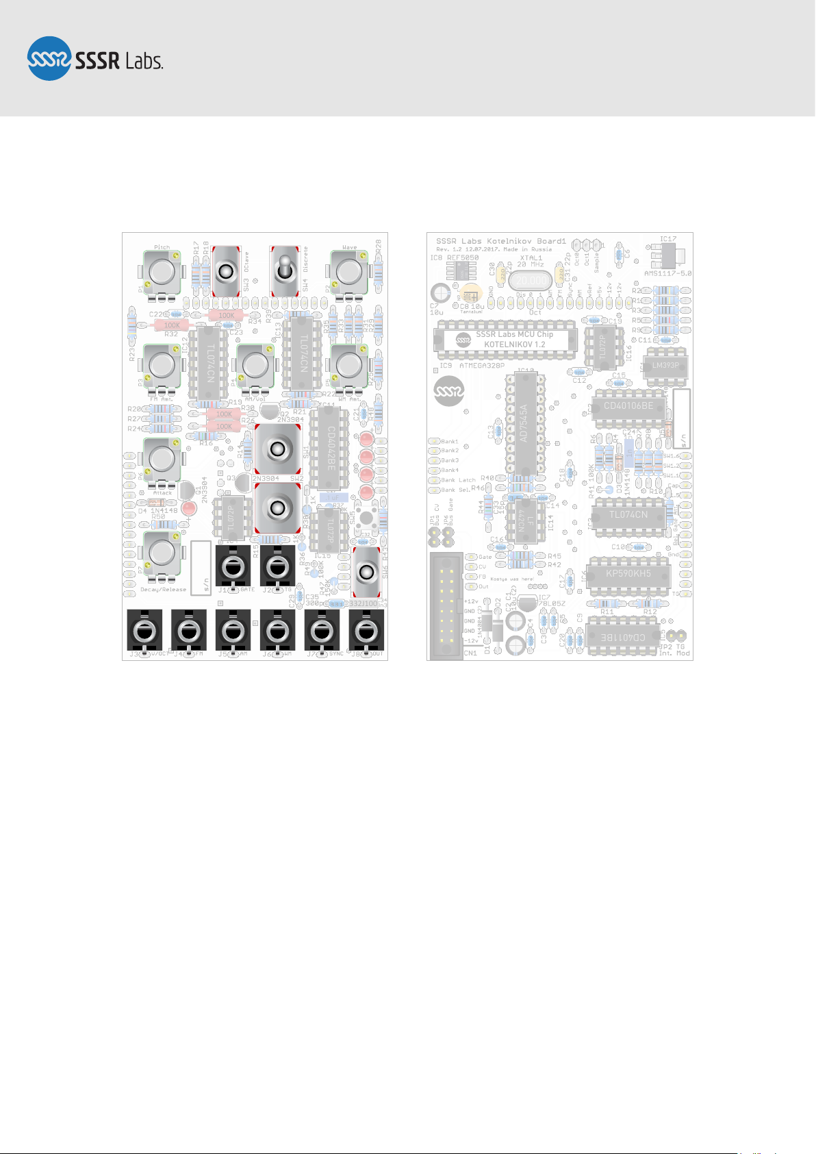
Step 12: Potentiometers, Switches, Jack Sockets
Install all potentiometers, toggle switches and jack sockets without washers and nuts.
Also, if there are fixing tabs on the potentiometers, you need to break them off with
pliers. The two 1M potentiometers must be installed in the TG area.
Page 13 of 18
Page 14
A TI REF
5050
220
220
.1 uF
332J100
20.000
TL074CN
TL074CN
TL074CN
CD4011BE
CD40106BE
TL072P
TL072P
TL072P
LM393P
LF
442CN
SSSR Labs MCU Chip
KOTELNIKOV 1.2
CD4042BE
KP590KH5
AD7545A
SM042, Assembly Manual
PCB Version 1.2
Step 13: Front Panel
Put on the panel back to its place. Since you do not longer need access to the top side
of the Board 2, you can put on and tighten all washers and nuts. Solder everything.
It is advisable to clean the Board 2 a second time, from the bottom side, but you must
do it carefully, avoiding moistening of the hardware. Any liquid inside the potentiometers, switches or jacks can cause serious performance degradation.
Page 14 of 18
Page 15
SM042, Assembly Manual
PCB Version 1.2
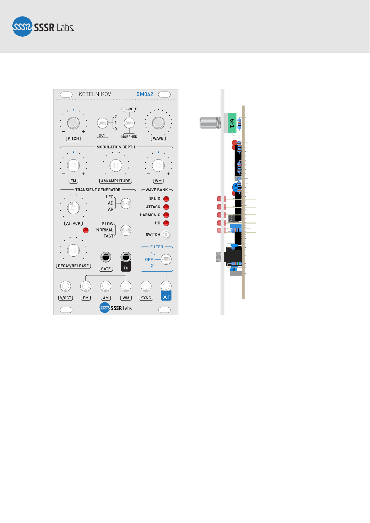
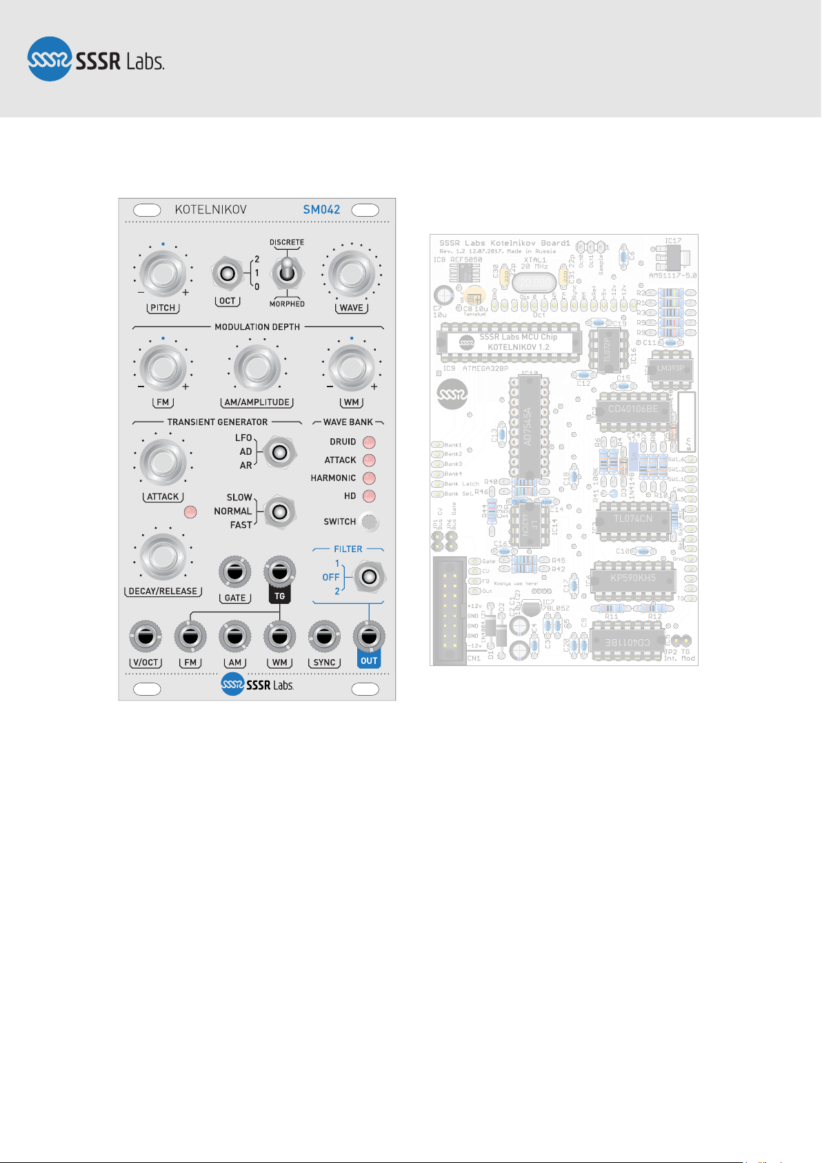
Step 14: First Power-On
The KOTELNIKOV module does not need any adjustment, but you can improve your
experience of using attenuverters if you're using round shafted potentiometers with
corresponding knobs.
Look over the module one more time and check everything you can.
Set the module to the settings pictured above. Connect the power, turn on your system
and make sure that DRUID indicator is on and TG LED is blinking. If it doesn't happen
for more than two seconds after powering-on, turn it off immediately and check for
build errors again.
If module is working as intended, you can proceed to knobs centering.
Page 15 of 18
Page 16

SM042, Assembly Manual
PCB Version 1.2
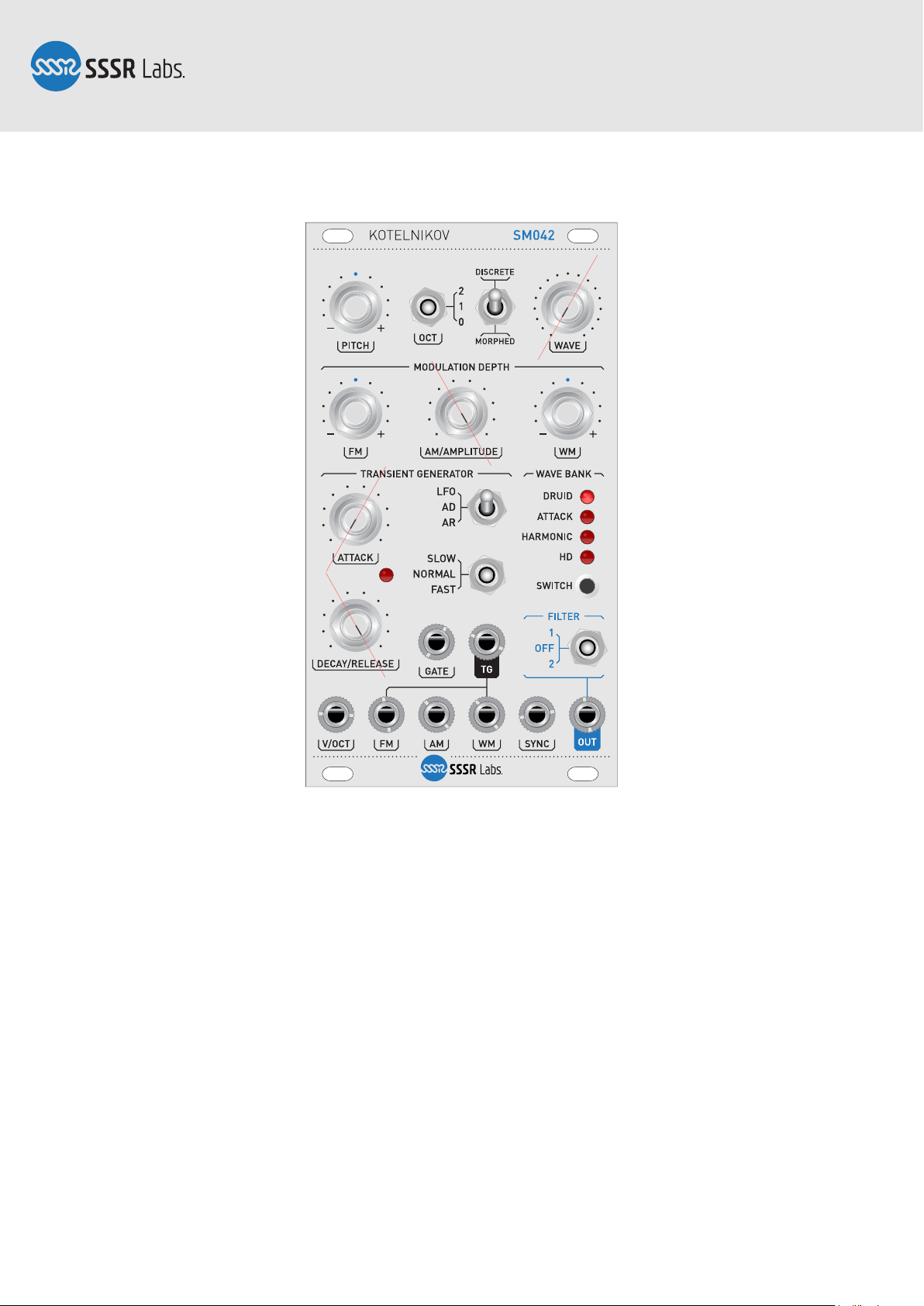
Step 15: Centering the Pitch Potentiometer
Prepare a thin permanent marker or a soft pencil. You are going to determine the
exact mid-points for all three polarized potentiometers.
For your convinience, you could also outline the pointer lines on the Wave, AM, Attack
and Decay shafts.
Set the module to the settings pictured above. Monitor the output frequency with an
oscilloscope, frequency meter, tuner or your ears and turn the Pitch shaft counterclockwise until the frequency stops changing. This will be the mid-point for the Pitch
knob. Now draw a straight line on the shaft's edge, pointing exactly to the top. Later,
this line will help you to put on the respective knob correctly.
Page 16 of 18
Page 17
SM042, Assembly Manual
PCB Version 1.2
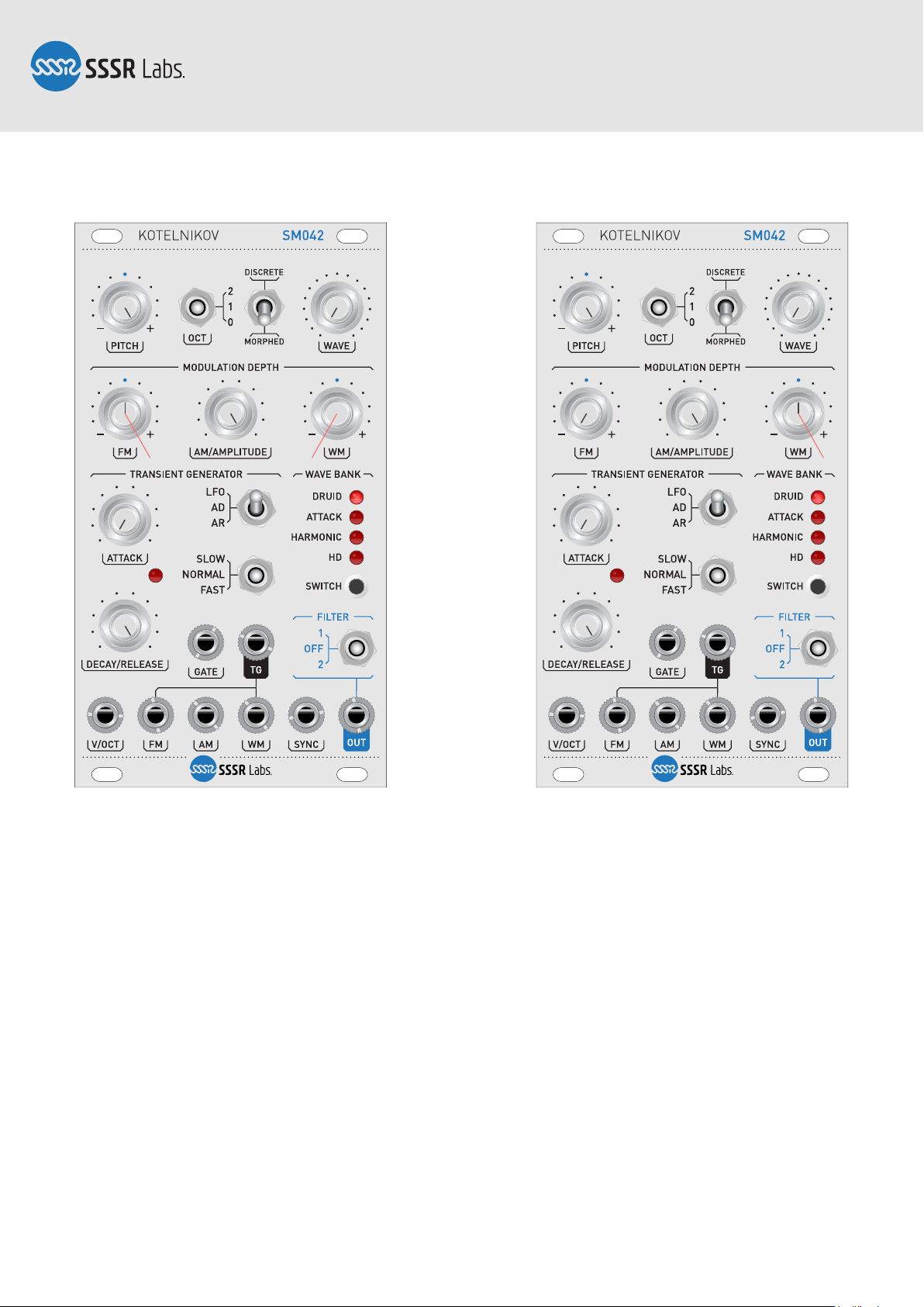
Step 16: Centering the FM and WM Potentiometers
Set the module to the settings shown on the left picture.
Module will sound like a kind of siren. Find the position of the FM shaft where frequency modulation is negligible or disappears completely. This is the mid-point for the
FM control. Outline the pointer line on this shaft.
Repeat this procedure with the WM shaft. The initial position is shown on the right
picture. The mid-point can be found using the similar procedure as for the FM shaft.
Page 17 of 18
Page 18
SM042, Assembly Manual
PCB Version 1.2
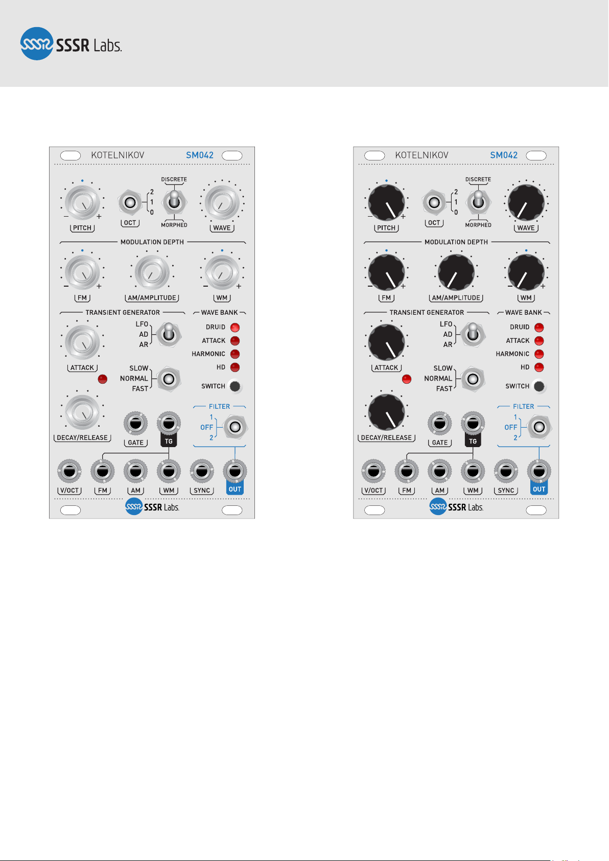
Step 17: Finishing the Build
Install the knobs. Some kits contain the D-Shaft sets of potentiometers and knobs.
Others contain the round shaft sets. If you have the round shaft set, you need to perform the following procedure. Turn all potentiometers to the position shown on the left
picture, then install each knob, one at a time, keeping it in the correct position. You
may also put the edge of a business card or other object of similar thickness under the
knob to make a little gap between the nut and the knob to prevent them from scraping
each other.
Once you have installed all knobs you are done building the module! Thank you for
purchasing an SSSR Labs product and we wish you to have a lot of fun with your new
module!
Page 18 of 18
 Loading...