

Page 1
Fixed or Adjustable Delays
0.1 s ...1000 m in 6 Ranges
+/-0.5% Repeat Accuracy
+/- 1% Factory Calibration
12 VDC...230 VAC in 5
Ranges
1 A Solid State Output
Encapsulated
Delay On Break (Release)Delay On Break (Release)
Delay On Break (Release)
Delay On Break (Release)Delay On Break (Release)
TSDB Series
Timing Module
DescriptionDescription
Description
DescriptionDescription
The TSD Series is designed for more demanding commercial and industrial applications where small size,
and accurate performance is required. The factory calibration for fixed time delays is within 1% of the target
time delay. The repeat accuracy, under stable conditions, is 0.5% of the time delay. The TSD Series is
rated to operate over an extended temperature range. Time delays of 0.1 seconds to 1000 minutes are
available. The output is rated 1 A steady and 10 A inrush. The modules are totally solid state and
encapsulated to protect the electronic circuitry.
OperationOperation
Operation
OperationOperation
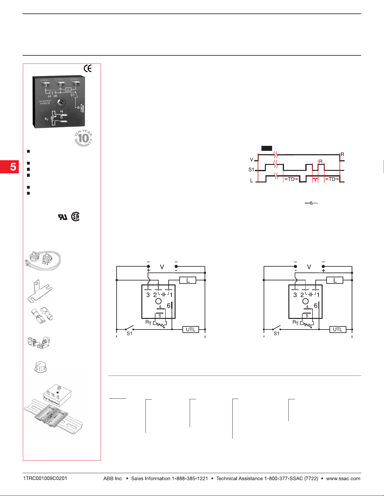
Input voltage must be applied before and during
timing. Upon closure of the initiate switch, the output
energizes. The time delay begins when the initiate
switch is opened. The output remains energized
during timing. At the end of the time delay, the output
de-energizes. The output will energize if the initiate
switch is closed when input voltage is applied.
Reset: Reset:
Reset: Reclosing the initiate switch during timing resets
Reset: Reset:
the time delay. Loss of input voltage resets the time
delay and output.
FunctionFunction
Function
FunctionFunction
Delay On Break
V = Voltage L = Load S1 = Initiate Switch
TD = Time Delay R = Reset
t = Incomplete Time Delay
= Undefined time
Approvals:
AccessoriesAccessories
Accessories
AccessoriesAccessories
BB
B
BB
→
DIN rail adaptor
P1023-20 P1023-20
P/N:
P1023-20
P1023-20 P1023-20
External adjust
potentiometer
AA
A
AA
P/Ns:
P1004-95P1004-95
P1004-95
P1004-95P1004-95
P1004-95-X P1004-95-X
P1004-95-X (fig B)
P1004-95-X P1004-95-X
Mounting bracket
P/N:
Female quick
connect
P/N
P1015-64P1015-64
P1015-64
P1015-64P1015-64
Quick connect to
screw adaptor
P/N:
Versa-knob
P/N:
DIN rail P/Ns:
017322005 017322005
017322005 (Steel)
017322005 017322005
C103PM C103PM
C103PM (Al)
C103PM C103PM
(fig A)
P1023-6 P1023-6
P1023-6
P1023-6 P1023-6
::
:
::
P1015-18 P1015-18
P1015-18
P1015-18 P1015-18
P0700-7 P0700-7
P0700-7
P0700-7 P0700-7
See accessory pages for
specifications.
(AWG 14/16)
←
ConnectionConnection
Connection
ConnectionConnection
OrOr
dering Tdering T
Or
dering T
OrOr
dering Tdering T
TSDBTSDB
TSDB
TSDBTSDB
SeriesSeries
Series
SeriesSeries
Example P/N: Example P/N:
Example P/N:
Example P/N: Example P/N:
Positive Switching
RT is used when external adjustment is ordered.
Dashed lines are internal connections.
UTL = Optional Untimed Load L = Timed Load S1 = Initiate Switch
ableable
able
ableable
X X
X
X X
InputInput
Input
InputInput
––
11
- -
–
1
- 12 V DC
––
11
- -
––
2 2
- -
–
2
- 24 V AC
––
2 2
- -
––
3 3
- -
–
3
- 24 V DC
––
3 3
- -
––
4 4
- -
–
4
- 120 V AC
––
4 4
- -
––
66
- -
–
6
- 230 V AC –
––
66
- -
TSDB420TSDB420
TSDB420 Fixed –
TSDB420TSDB420
X X
X
X X
Adjustment Adjustment
Adjustment
Adjustment Adjustment
––
11
- -
–
1
-
––
11
- -
Fixed
––
22
- -
–
2
-
––
22
- -
External
Adjust
––
33
- -
–
3
-
––
33
- -
Onboard
Adjust
TSDB110.1SPTSDB110.1SP
TSDB110.1SP
TSDB110.1SPTSDB110.1SP
X X
X
X X
Time Delay*Time Delay*
Time Delay*
Time Delay*Time Delay*
––
00
- -
–
0
- 0.1 … 10 s
––
00
- -
––
11
--
–
1
- 1 … 100 s –
––
11
--
––
22
- -
–
2
- 10 … 1000 s –
––
22
- -
––
33
- -
–
3
- 0.1 … 10 m
––
33
- -
44
4 - 1 ... 100 m
44
55
--
–
5
- 10 … 1000 m
55
--
Negative Switching
X X
X
X X
Switching ModeSwitching Mode
Switching Mode
Switching ModeSwitching Mode
(V DC Only)(V DC Only)
(V DC Only)
(V DC Only)(V DC Only)
PP
P
-
PP
Positive
NN
N
-
NN
Negative
* If Fixed Delay is selected, insert
0.10.1
delay [
SS
(
S) sec. or (
SS
10001000
0.1 …
1000] followed by
0.10.1
10001000
MM
M) min.
MM
TSDBGen 07.01.04
Low Voltage Products & Systems5.66
Page 2
Delay On Break (Release)Delay On Break (Release)
Delay On Break (Release)
Delay On Break (Release)Delay On Break (Release)
TSDB Series
Timing Module
Technical DataTechnical Data
Technical Data
Technical DataTechnical Data
Time DelayTime Delay
Time Delay
Time DelayTime Delay
Range 0.1 s ... 1000 m in 6 adjustable ranges or fixed
Repeat Accuracy +/-0.5 % or 20 ms, whichever is greater
Tolerance (Factory Calibration) ≤ +/-1%
Reset Time ≤ 150 ms
Initiate Time ≤ 20 ms
Time Delay vs. Temperature & Voltage ≤ +/-2%
InputInput
Input
InputInput
Voltage 12 or 24 V DC; 24, 120, or 230 V AC
Tolerance +/-15%
Power Consumption AC ≤ 2 VA; DC ≤ 1 W
Line Frequency 50 ... 60 Hz
DC Ripple ≤ 10 %
OutputOutput
Output
OutputOutput
Type Solid state
Form Normally Open, closed before & during timing
Maximum Load Current 1 A steady state, 10 A inrush at 60°C
Off State Leakage Current ≅ 5 mA at 230 V AC; DC ≅ 1 mA
Voltage Drop AC ≅ 2.5 V at 1 A; DC ≅ 1 V at 1 A
DC Operation Positive or negative switching
ProtectionProtection
Protection
ProtectionProtection
Circuitry Encapsulated
Dielectric Breakdown ≥ 2000 V RMS terminals to mounting surface
Insulation Resistance ≥ 100 MΩ
Polarity DC units are reverse polarity protected
MechanicalMechanical
Mechanical
MechanicalMechanical
Mounting Surface mount with one #10 (M5 x 0.8) screw
Termination 0.25 in. (6.35 mm) male quick connect terminals
EnvironmentalEnvironmental
Environmental
EnvironmentalEnvironmental
Operating/Storage Temperature -40°C ... +75°C / -40°C ... +85°C
Humidity 95% relative, non-condensing
Weight ≅ 2.4 oz (68 g)
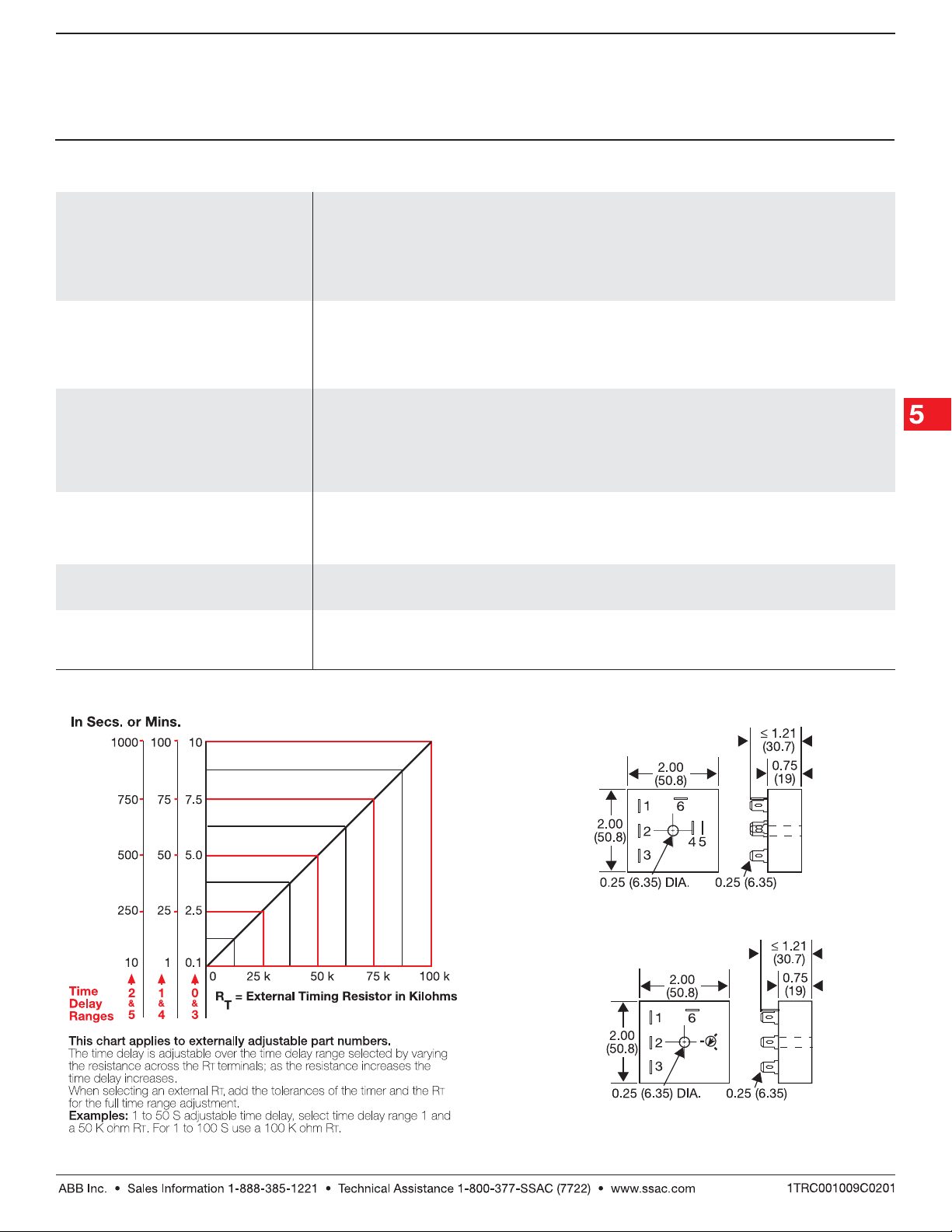
External Resistance vs Time DelayExternal Resistance vs Time Delay
External Resistance vs Time Delay
External Resistance vs Time DelayExternal Resistance vs Time Delay
TSDBGen 07.01.04
Mechanical ViewMechanical View
Mechanical View
Mechanical ViewMechanical View
Fixed and External AdjustFixed and External Adjust
Fixed and External Adjust
Fixed and External AdjustFixed and External Adjust
Onboard AdjustOnboard Adjust
Onboard Adjust
Onboard AdjustOnboard Adjust
Inches (Millimeters)
Low Voltage Products & Systems 5.67
 Loading...