

Page 1

Operation and Service Manual
Stanford Research Systems
Analog Limiter
SIM964
Revision 1.4 • August 28, 2006
Page 2

Certification
Stanford Research Systems certifies that this product met its published specifications at the time
of shipment.
Warranty
This Stanford Research Systems product is warranted against defects in materials and workmanship for a period of one (1) year from the date of shipment.
Service
For warranty service or repair, this product must be returned to a Stanford Research Systems
authorized service facility. Contact Stanford Research Systems or an authorized representative
before returning this product for repair.
Information in this document is subject to change without notice.
Copyrightc Stanford Research Systems, Inc., 2006. All rights reserved.
Stanford Research Systems, Inc.
1290–D Reamwood Avenue
Sunnyvale, CA 94089 USA
Phone: (408) 744-9040 • Fax: (408) 744-9049
www.thinkSRS.com • e-mail: info@thinkSRS.com
Printed in U.S.A. Document number 9-01599-903
SIM964 Analog Limiter
Page 3

Contents
General Information iii
Safety and Preparation for Use . . . . . . . . . . . . . . . . iii
Symbols . . . . . . . . . . . . . . . . . . . . . . . . . . . . . iv
Notation . . . . . . . . . . . . . . . . . . . . . . . . . . . . . v
Specifications . . . . . . . . . . . . . . . . . . . . . . . . . . vi
1 Getting Started 1 – 1
1.1 Overview . . . . . . . . . . . . . . . . . . . . . . . . . . 1– 2
1.2 Front-panel Operation . . . . . . . . . . . . . . . . . . 1 –3
1.3 Clock Stopping . . . . . . . . . . . . . . . . . . . . . . 1 –5
1.4 SIM Interface . . . . . . . . . . . . . . . . . . . . . . . . 1 – 6
2 Remote Operation 2 – 1
2.1 Index of Common Commands . . . . . . . . . . . . . . 2 – 2
2.2 Alphabetic List of Commands . . . . . . . . . . . . . . 2– 4
2.3 Introduction . . . . . . . . . . . . . . . . . . . . . . . . 2– 5
2.4 Commands . . . . . . . . . . . . . . . . . . . . . . . . . 2 – 5
2.5 Status Model . . . . . . . . . . . . . . . . . . . . . . . . 2 – 15
3 Circuitry 3 – 1
3.1 Circuit Descriptions . . . . . . . . . . . . . . . . . . . . 3– 2
3.2 Parts Lists . . . . . . . . . . . . . . . . . . . . . . . . . 3 – 5
3.3 Schematic Diagrams . . . . . . . . . . . . . . . . . . . 3 – 6
i
Page 4

ii Contents
SIM964 Analog Limiter
Page 5

General Information
The SIM964 Analog Limiter, part of Stanford Research Systems’
Small Instrumentation Modules family, is a low-noise programmable
clamp for general signal conditioning from DC to 1 MHz. Upper and
lower limits are independently settable between ±10 V with 10 mV
resolution. The clamped signal is available at the front-panel output,
while rear-panel logic outputs indicate when either limit is exceeded.
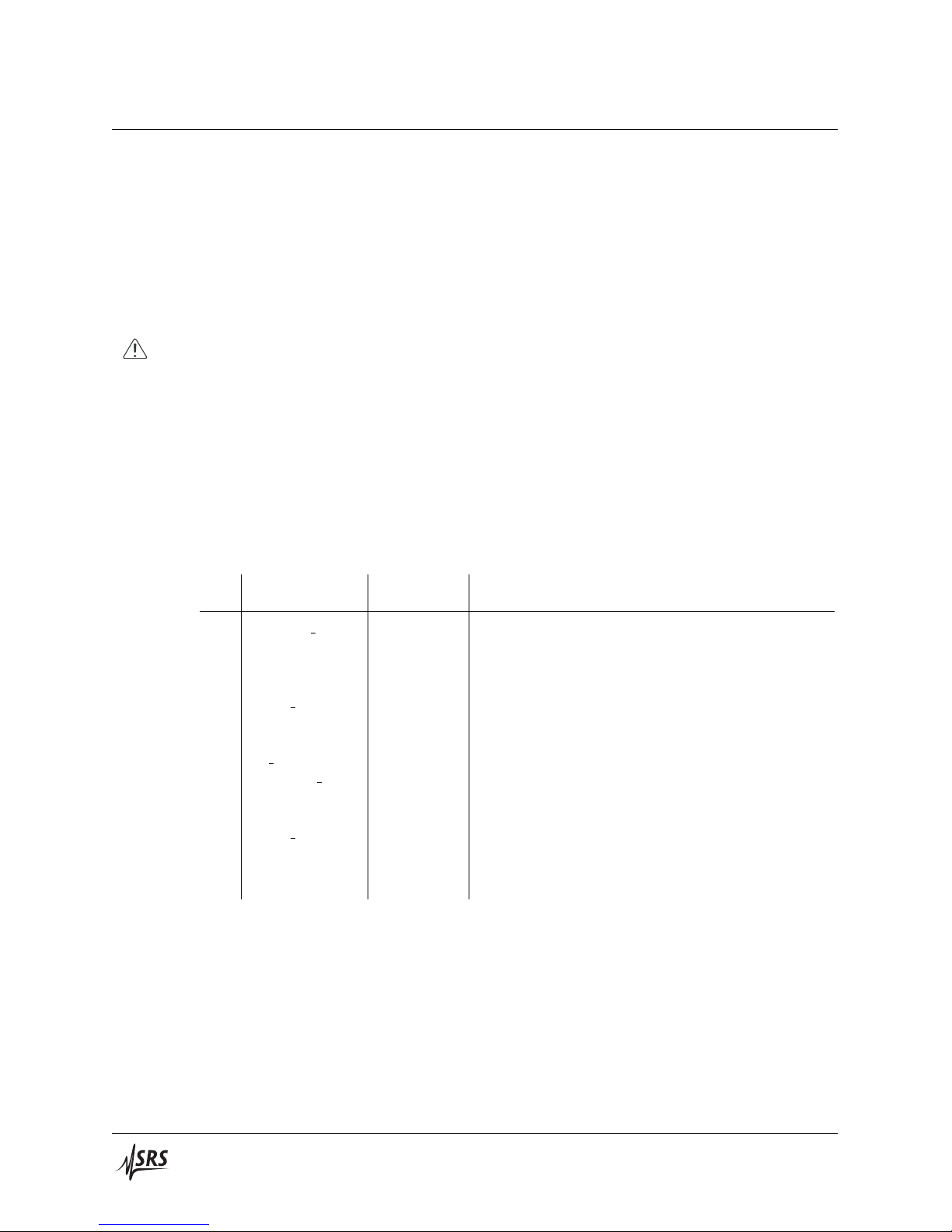
Safety and Preparation for Use
The front-panel input, front-panel output, and the rear-panel output
coaxial (BNC) connectors in the SIM964 are referenced to the Earth,
and their outer casings are grounded. No dangerous voltages are
generated by the module.
WARNING
Do not exceed ±15 volts to the Earth at the center terminal of any BNC
connector. Do not install substitute parts or perform any unauthorized
modifications to this instrument.
The SIM964 is a single-wide module designed to be used inside the
SIM900 Mainframe. Do not turn on the power until the module is
completely inserted into the mainframe and locked in place.
iii
Page 6

iv General Information
Symbol Description
Alternating current
Caution - risk of electric shock
Frame or chassis terminal
Caution - refer to accompanying documents
Earth (ground) terminal
Battery
Fuse
On (supply)
Off (supply)
Symbols you may Find on SRS Products
SIM964 Analog Limiter
Page 7

General Information v
Notation
The following notation will be used throughout this manual.
WARNING
CAUTION
A warning means that injury or death is possible if the instructions
are not obeyed.
A caution means that damage to the instrument or other equipment
is possible.
Typesetting conventions used in this manual are:
• Front-panel buttons are set as [Button];
[Adjust ] is shorthand for “[Adjust ] & [Adjust ]”.
• Front-panel indicators are set as Overload.
• Remote command names are set as *IDN?.
• Literal text other than command names is set as OFF.
Remote command examples will all be set in monospaced font. In
these examples, data sent by the host computer to the SIM964 are set
as straight teletype font, while responses received by the host
computer from the SIM964 are set as slanted teletype font.
SIM964 Analog Limiter
Page 8

vi General Information
Specifications
Performance Characteristics
Limit setting range ±10 V
Resolution 10 mV
Bandwidth 1 MHz
Gain 1×
Input impedance 1 MΩ
Output noise < 400 µV rms
Total harmonic distortion 0.01 % (−80 dB) at 1 kHz
Slew rate 70 V/µs
Limit detection TTL level outputs are when
corresponding limit (upper/lower) is exceeded.
Operating temperature 0◦C to 40◦C, non-condensing
Power +5 V (50 mA typ., 100 mA max.)
±15 V (50 mA typ., 300 mA max.)
General Characteristics
Interface Serial (RS-232) through SIM interface
Connectors BNC (2 front, 2 rear)
DB–15 (male) SIM interface
Weight 1.5 lbs
Dimensions 1.500W × 3.600H × 7.000D
SIM964 Analog Limiter
Page 9

1 Getting Started
In This Chapter
This chapter gives you the necessary information to get started
quickly with the SIM964 Analog Limiter.
1.1 Overview . . . . . . . . . . . . . . . . . . . . . . . . 1 – 2
1.2 Front-panel Operation . . . . . . . . . . . . . . . . . 1 – 3
1.2.1 Upper limit . . . . . . . . . . . . . . . . . . . 1 – 3
1.2.2 Lower limit . . . . . . . . . . . . . . . . . . . 1 – 3
1.2.3 Shortcuts . . . . . . . . . . . . . . . . . . . . . 1 – 4
1.2.4 Input . . . . . . . . . . . . . . . . . . . . . . . 1 – 4
1.2.5 Output . . . . . . . . . . . . . . . . . . . . . . 1 – 4
1.2.6 Rear panel outputs . . . . . . . . . . . . . . . 1 – 4
1.3 Clock Stopping . . . . . . . . . . . . . . . . . . . . . 1 – 5
1.4 SIM Interface . . . . . . . . . . . . . . . . . . . . . . 1 – 6
1.4.1 SIM interface connector . . . . . . . . . . . . 1 – 6
1.4.2 Direct interfacing . . . . . . . . . . . . . . . . 1 – 6
1 – 1
Page 10

1 – 2 Getting Started
1.1 Overview
The SIM964 Analog Limiter is a digitally programmable signal limiter with a fully analog signal path. User-defined upper and lower
voltage limits, in the range of ±10 V, define a linear operating band
for input signals from DC to 1 MHz.
The user can select an upper voltage limit, VUL, and a lower voltage
limit, VLL, either remotely, or from the front panel. While the input
signal, Vi, is within the range defined by the upper and lower limits,
the SIM964 output, Vo, is a unity-gain buffered signal that follows the
input signal. If the input signal exceeds one of the limits, the output
of the SIM964 will be clamped to that limit for as long as the signal
is in excess of the limit. When the input signal returns to the range
between the limits, the output immediately recovers and follows the
input signal again.
Mathematically, this can be expressed as
V
UL
V
i
V
LL
Vi> V
UL
VUL≥ Vi≥ V
Vi< V
LL
LL
Vo=
The input and output signals are applied to the SIM964 through
BNC connections on the front panel. Two TTL monitor outputs,
corresponding to upper and lower limit saturation conditions, are
provided through rear-panel BNC connections. The TTL output
level is +5 V when the corresponding limit is not exceeded, and falls
to 0 V for as long as the input is in excess of the limit.
SIM964 Analog Limiter
Page 11

1.2 Front-panel Operation 1 – 3
1.2 Front-panel Operation
The front panel of the SIM964 (see Figure 1.1) provides a simple
operator interface.
1.2.1 Upper limit
1.2.2 Lower limit
Figure 1.1: The SIM964 front and rear panels.
The [ ] and [ ] buttons on the left side of the front panel are associated
with the upper numeric display to form the Upper Limit block. The
numeric display indicates the value of VUL(in volts), with 10 mV
resolution.
Pressing [UL ] will raise the upper voltage limit, while [UL ] will
lower it. Short presses of either key will step the limit in 10 mV
increments; holding the key continuously will cause the limit setting
to continuously change upwards or downwards at an accelerating
rate.
The upper limit voltage VULcan be set within the range:
+10 V ≥ VUL≥ (VLL+ 100 mV)
The [ ] and [ ] buttons on the right side of the front panel are associated with the lower numeric display to form the Lower Limit block.
SIM964 Analog Limiter
Page 12

1 – 4 Getting Started
Operation is analogous to the Upper Limit block. Note, however,
that pressing [LL ] will increase the signed value of VLL(that is,
make VLLmore positive); this acts to narrow the linear range of the
SIM964, rather than expand it.
The lower limit voltage VLLcan be set within the range:
(VUL− 100 mV) ≥ VLL≥ −10 V
1.2.3 Shortcuts
Pressing the two buttons [UL ] simultaneously will step the VULsetting between +10 V, +5 V, 0 V, and −5 V (each successive two-button
press steps to the next setting). This shortcut, however, cannot set
VUL< (VLL+ 100 mV). Similarly, pressing the two buttons [LL
simultaneously will step the VLLsetting between −10 V, −5 V, 0 V,
and +5 V.
1.2.4 Input
The user signal, Vi, is input at the front-panel upper BNC connector,
which presents a 1 MΩ input impedance.
]
1.2.5 Output
1.2.6 Rear panel outputs
The analog output, Vo, is available at the front-panel lower BNC
connector. Note that the SIM964 has a 50 Ω output impedance. When
driving an external 50 Ω user load, this will result in the output signal
being divided by 2.
The two BNC connectors on the rear panel provide TTL monitor
signals for the state of the SIM964 Analog Limiter. When the upper
or lower limit is exceeded, the corresponding rear panel output is
(0 V); otherwise it idles (+5 V).
SIM964 Analog Limiter
Page 13

1.3 Clock Stopping 1 – 5
1.3 Clock Stopping
The microprocessor clock of the SIM964 stops if the module is idle,
“freezing” the digital circuitry. The following actions “wake up” the
clock:
1. A power-on.
2. A press of a front-panel button.
3. Activity (send or receive) at the remote interface.
4. An input overload.
5. An upper or lower limit clamp.
The clock runs for as long as is necessary to complete a limit setting
adjustment, or to communicate the output of a query through the
remote interface. However, the clock will remain active for as long
as the overload or limit condition exists.
This default behavior can be modified with the remote com-
mand AWAK. Setting AWAKON will prevent the clock from stopping.
The module returns to AWAKOFF upon power-on.
SIM964 Analog Limiter
Page 14
1 – 6 Getting Started
1.4 SIM Interface
The primary connection to the SIM964 Analog Limiter is the rearpanel DB–15 SIM interface connector. Typically, the SIM964 is mated
to a SIM900 Mainframe via this connection, either through one of the
internal Mainframe slots, or the remote cable interface.
It is also possible to operate the SIM964 directly, without using the
SIM900 Mainframe. This section provides details on the interface.
CAUTION
The SIM964 has no internal protection against reverse polarity, missing
supply, or overvoltage on the power supply pins. Misapplication of power
may cause circuit damage. SRS recommends using the SIM964 together
with the SIM900 Mainframe for most applications.
1.4.1 SIM interface connector
The DB–15 SIM interface connector carries all the power and communications lines to the instrument. The connector signals are specified
in Table 1.1
Pin Signal Src ⇒ Dest Description
1 SIGNAL GND MF ⇒ SIM Ground reference for signal
2 −STATUS SIM ⇒ MF Status/service request (GND = asserted, +5 V= idle)
3 RTS MF ⇒ SIM HW handshake (unused in SIM964)
4 CTS SIM ⇒ MF HW handshake (unused in SIM964)
5 −REF 10MHZ MF ⇒ SIM 10 MHz reference (no connection in SIM964)
6 −5 V MF ⇒ SIM Power supply (no connection in SIM964)
7 −15 V MF ⇒ SIM Power supply
8 PS RTN MF ⇒ SIM Power supply return
9 CHASSIS GND Chassis ground
10 TXD MF ⇒ SIM Async data (start bit = “0”= +5 V; “1” = GND)
11 RXD SIM ⇒ MF Async data (start bit = “0”= +5 V; “1” = GND)
12 +REF 10MHz MF ⇒ SIM 10 MHz reference (no connection in SIM964)
13 +5 V MF ⇒ SIM Power supply
14
+15 V MF ⇒ SIM Power supply
15 +24 V MF ⇒ SIM Power supply (no connection in SIM964)
Direction
1.4.2 Direct interfacing
Table 1.1: SIM Interface Connector Pin Assignments, DB-15
The SIM964 is intended for operation in the SIM900 Mainframe, but
users may wish to directly interface the module to their own systems
without the use of additional hardware.
SIM964 Analog Limiter
Page 15

1.4 SIM Interface 1 – 7
The mating connector needed is a standard DB–15 receptacle, such as
Amp part # 747909-2 (or equivalent). Clean, well-regulated supply
voltages of ±15,+5VDC must be provided, following the pin-out
specified in Table 1.1. Ground must be provided on pins 1 and 8,
with chassis ground on pin 9. The −STATUSsignal may be monitored
on pin 2 for a low-going TTL-compatible output indicating a status
message.
1.4.2.1 Direct interface cabling
If the user intends to directly wire the SIM964 independent of the
SIM900 Mainframe, communication is usually possible by directly
connecting the appropriate interface lines from the SIM964 DB–15
plug to the RS-232 serial port of a personal computer.1Connect RXD
from the SIM964 directly to RD on the PC, TXD directly to TD. In
other words, a null-modem style cable is not needed.
To interface directly to the DB–9 male (DTE) RS-232 port typically
found on contemporary personal computers, a cable must be made
with a female DB–15 socket to mate with the SIM964, and a female
DB–9 socket to mate with the PC’s serial port. Separate leads from
the DB–15 need to go to the power supply, making what is sometimes
know as a “hydra” cable. The pin-connections are given in Table 1.2.
DB–15/F to SIM964 Name
DB–9/F
10 ←→ 3 TxD
11 ←→ 2 RxD
5 Computer Ground
to P/S
7 ←→ −15 VDC
13 ←→ +5 VDC
14 ←→ +15 VDC
8,9 ←→ Ground (P/S return current)
1 ←→ Signal Ground (separate wire to Ground)
Table 1.2: SIM964 Direct Interface Cable Pin Assignments
1
Although the serial interface lines on the DB-15 do not satisfy the minimum
voltage levels of the RS-232 standard, they are typically compatible with desktop
personal computers
SIM964 Analog Limiter
Page 16

1 – 8 Getting Started
1.4.2.2 Serial settings
The initial serial port settings at power-on are: 9600 Baud, 8–bits, no
parity, 1 stop bit, and no flow control. The serial baud rate is fixed,
but the parity may be changed with the PARI commands.
SIM964 Analog Limiter
Page 17

2 Remote Operation
In This Chapter
This chapter describes operating the SIM964 over the serial interface.
2.1 Index of Common Commands . . . . . . . . . . . . 2 – 2
2.2 Alphabetic List of Commands . . . . . . . . . . . . 2 – 4
2.3 Introduction . . . . . . . . . . . . . . . . . . . . . . . 2 – 5
2.3.1 Power-on configuration . . . . . . . . . . . . 2 – 5
2.3.2 Buffers . . . . . . . . . . . . . . . . . . . . . . 2 – 5
2.3.3 Device Clear . . . . . . . . . . . . . . . . . . . 2 – 5
2.4 Commands . . . . . . . . . . . . . . . . . . . . . . . 2 – 5
2.4.1 Command Syntax . . . . . . . . . . . . . . . . 2 – 6
2.4.2 Notation . . . . . . . . . . . . . . . . . . . . . 2 – 7
2.4.3 Examples . . . . . . . . . . . . . . . . . . . . 2 – 7
2.4.4 Configuration Commands . . . . . . . . . . . 2 – 8
2.4.5 Monitor Commands . . . . . . . . . . . . . . 2 – 9
2.4.6 Serial Communication Commands . . . . . . 2 – 9
2.4.7 Status Commands . . . . . . . . . . . . . . . 2 – 10
2.4.8 Interface Commands . . . . . . . . . . . . . . 2 – 11
2.5 Status Model . . . . . . . . . . . . . . . . . . . . . . 2 – 15
2.5.1 Status Byte (SB) . . . . . . . . . . . . . . . . . 2 – 16
2.5.2 Service Request Enable (SRE) . . . . . . . . . 2 – 17
2.5.3 Standard Event Status (ESR) . . . . . . . . . 2 – 17
2.5.4 Standard Event Status Enable (ESE) . . . . . 2 – 18
2.5.5 Communication Error Status (CESR) . . . . . 2 – 18
2.5.6 Communication Error Status Enable (CESE) 2 – 19
2 – 1
Page 18

2 – 2 Remote Operation
2.1 Index of Common Commands
symbol definition
i,j Integers
f Floating-point values
z Literal token
(?) Required for queries; illegal for set commands
var parameter always required
{var} required parameter for set commands; illegal for queries
[var] optional parameter for both set and query forms
Configuration
ULIM(?) {f } 2 – 8 Upper Limit
LLIM(?) {f } 2 – 8 Lower Limit
AWAK(?) {z} 2 – 8 Keep Clock Awake
Monitor
ULCR? 2 – 9 Upper Limit Condition
LLCR? 2 – 9 Lower Limit Condition
OVLD? 2 – 9 Overload Condition
Serial Communications
PARI(?) {z} 2 – 9 Parity
Status
*STB? [i] 2 – 10 Status Byte
*SRE(?) [i,] {j} 2 – 10 Service Request Enable
*CLS 2 – 10 Clear Status
*ESR? [i] 2 – 10 Standard Event Status
*ESE(?) [i,] {j} 2 – 10 Standard Event Status Enable
CESR? [i] 2 – 11 Comm Error Status
CESE(?) [i,]{j} 2 – 11 Comm Error Status Enable
PSTA(?) {z} 2 – 11 Pulse −STATUS Mode
Interface
*RST 2 – 11 Reset
*IDN? 2 – 12 Identify
*OPC(?) 2 – 12 Operation Complete
CONS(?) {z} 2 – 12 Console Mode
LEXE? 2 – 12 Execution Error
LCME? 2 – 13 Command Error
LBTN? 2 – 13 Button
TOKN(?) {z} 2 – 14 Token Mode
TERM(?) {z} 2 – 14 Response Termination
SIM964 Analog Limiter
Page 19

2.1 Index of Common Commands 2 – 3
SIM964 Analog Limiter
Page 20

2 – 4 Remote Operation
2.2 Alphabetic List of Commands
?
*CLS 2 – 10 Clear Status
*ESE(?) [i,] {j} 2 – 10 Standard Event Status Enable
*ESR? [i] 2 – 10 Standard Event Status
*IDN? 2 – 12 Identify
*OPC(?) 2 – 12 Operation Complete
*RST 2 – 11 Reset
*SRE(?) [i,] {j} 2 – 10 Service Request Enable
*STB? [i] 2 – 10 Status Byte
A
AWAK(?) {z} 2 – 8 Keep Clock Awake
C
CESE(?) [i,]{j} 2 – 11 Comm Error Status Enable
CESR? [i] 2 – 11 Comm Error Status
CONS(?) {z} 2 – 12 Console Mode
L
LBTN? 2 – 13 Button
LCME? 2 – 13 Command Error
LEXE? 2 – 12 Execution Error
LLCR? 2 – 9 Lower Limit Condition
LLIM(?) {f } 2 – 8 Lower Limit
O
OVLD? 2 – 9 Overload Condition
P
PARI(?) {z} 2 – 9 Parity
PSTA(?) {z} 2 – 11 Pulse −STATUS Mode
T
TERM(?) {z} 2 – 14 Response Termination
TOKN(?) {z} 2 – 14 Token Mode
U
ULCR? 2 – 9 Upper Limit Condition
ULIM(?) {f } 2 – 8 Upper Limit
SIM964 Analog Limiter
Page 21

2.3 Introduction 2 – 5
2.3 Introduction
Remote operation of the SIM964 is through a simple command language documented in this chapter. Both set and query forms of
most commands are supported, allowing the user complete control
of the analog limiter from a remote computer, either through the
SIM900 Mainframe or directly via RS-232 (see Section 1.4.2.1).
See Table 1.1 for specification of the DB–15 SIM interface connector.
2.3.1 Power-on configuration
The settings for the remote interface are 9600 baud with no parity or
flow control, and local echo disabled (CONS OFF).
Most of the SIM964 instrument settings are stored in non-volatile
memory, and at power-on the instrument returns to the state it was
last in when power was removed. Exceptions are noted in the command descriptions.
Reset values of parameters are shown in boldface.
2.3.2 Buffers
2.3.3 Device Clear
Incoming data from the host interface is stored in a 64-byte input
buffer. Characters accumulate in the input buffer until a command
terminator (either hCRi or hLFi) is received, at which point the message is parsed and executed. Query responses from the SIM964 are
buffered in a 64-byte output queue.
If the input buffer overflows, then all data in both the input buffer
and the output queue are discarded, and an error is recorded in the
CESR and ESR status registers.
The SIM964 host interface can be asynchronously reset to its poweron configuration by sending an RS-232-style hbreaki signal. From
the SIM900 Mainframe, this is accomplished with the SIM900 SRST
command; if directly interfacing via RS-232, then use a serial break
signal. After receiving the Device Clear, the interface is reset to 9600
baud and CONS mode is turned OFF. Note that this only resets the
communication interface; the basic function of the SIM964 is left
unchanged; to reset the instrument, see *RST.
2.4 Commands
SIM964 Analog Limiter
This section provides syntax and operational descriptions for reomote commands.
Page 22

2 – 6 Remote Operation
2.4.1 Command Syntax
The four letter mnemonic (shown in CAPS) in each command se-
quence specifies the command. The rest of the sequence consists of
parameters.
Commands may take either set or query form, depending on whether
the “?” character follows the mnemonic. Set only commands are
listed without the “?”, query only commands show the “?” after the
mnemonic, and optionally query commands are marked with a “(?)”.
Parameters shown in { } and [ ] arenot always required. Parameters in
{ } are required to set a value, and are omitted for queries. Parameters
in [ ] are optional in both set and query commands. Parameters listed
without any surrounding characters are always required.
Do not send ( ) or { } or [ ] as part of the command.
Multiple parameters are separated by commas. Multiple commands
may be sent on one command line by separating them with semicolons (;) so long as the input buffer does not overflow. Commands
are terminated by either hCRi or hLFi characters. Null commands
and whitespace are ignored. Execution of command(s) does not
begin until the command terminator is received.
Token parameters (generically shown as z in the command de-tokens
scriptions) can be specified either as a keyword or integer value.
Command descriptions list the valid keyword options, with each
keyword followed by its corresponding integer value. For example,
to set the response termination sequence to hCRi+hLFi, the following
two commands are equivalent:
TERM CRLF —or— TERM 3
For queries that return token values, the return format (keyword or
integer) is specified with the TOKN command.
SIM964 Analog Limiter
Page 23

2.4 Commands 2 – 7
2.4.2 Notation
The following table summarizes the notation used in the command
descriptions:
symbol definition
i,j Integers
f Floating-point values
z Literal token
(?) Required for queries; illegal for set commands
var parameter always required
{var} required parameter for set commands; illegal for queries
[var] optional parameter for both set and query forms
2.4.3 Examples
Each command is provided with a simple example illustrating its
usage. In these examples, all data sent by the host computer to
the SIM964 are set as straight teletype font, while responses
received the host computer from the SIM964 are set as slanted
teletype font.
The usage examples vary with respect to set/query, optional parameters, and token formats. These examples are not exhaustive, but are
intended to provide a convenient starting point for user programming.
SIM964 Analog Limiter
Page 24

2 – 8 Remote Operation
2.4.4 Configuration Commands
Upper LimitULIM(?) {f }
Set (query) the upper limit voltage VUL{to f}, in volts.
If ULIM is set outside the range
+10 V ≥ VUL≥ VLL+ 100 mV,
then the command will fail, setting the EXE bit in the *ESR register,
and setting the LEXE parameter to “invalid parameter” (16).
ULIM 3.14Example:
ULIM?
+3.14
Lower LimitLLIM(?) {f}
Set (query) the lower limit voltage VLL{to f}, in volts.
If LLIM is set outside the range
VUL− 100 mV ≥ VLL≥ −10 V,
then the command will fail, setting the EXE bit in the *ESR register,
and setting the LEXE parameter to “invalid parameter” (16).
LLIM -8.042Example:
LLIM?
-8.04
Keep Clock AwakeAWAK(?) {z}
Set (query) the SIM964 keep-awake mode {to z = (OFF 0, ON 1)}.
Ordinarily, the clock oscillator for the SIM964 microcontroller is held
in a stopped state, and only enabled during processing of events
(Section 1.3). Setting AWAK ON forces the clock to stay running, and
is useful only for diagnostic purposes.
AWAK ONExample:
SIM964 Analog Limiter
Page 25

2.4 Commands 2 – 9
2.4.5 Monitor Commands
Upper Limit ConditionULCR?
Query the upper limit detector. Returns 1 if input signal exceeds the
upper limit voltage, Vi> VUL. Returns 0 otherwise.
ULCR? returns the complement of the rear-panel output; ULCR?
returns 1 when the Upper Limit Detect output is , and 0 when
.
ULCR?Example:
0
Lower Limit ConditionLLCR?
Query the lower limit detector. Returns 1 if input signal exceeds the
lower limit voltage, Vi< VLL. Returns 0 otherwise.
LLCR? returns the complement of the rear-panel output; LLCR?
returns 1 when the Lower Limit Detect output is , and 0 when
.
LLCR?Example:
1
Overload ConditionOVLD?
Query the input overload detector. Returns 1 if the input is overloaded, or 0 otherwise.
OVLD?Example:
0
2.4.6 Serial Communication Commands
ParityPARI(?) {z}
Set (query) parity {to z = (NONE 0, ODD 1, EVEN 2, MARK 3, SPACE 4)}.
After power-on, modules default to PARI NONE.
PARI EVENExample:
SIM964 Analog Limiter
Page 26

2 – 10 Remote Operation
2.4.7 Status Commands
The Status commands query and configure registers associated with
status reporting of the SIM964.
Status Byte*STB? [i]
Reads the Status Byte register [bit i].
Execution of the *STB?query (without the optinal bit i) always causes
the −STATUS signal to be deasserted. Note that *STB? i will not clear
−STATUS, even if bit i is the only bit presently causing the −STATUS
signal. See also the PSTA command.
*STB?Example:
16
Service Request Enable*SRE(?) [i,] {j}
Set (query) the Service Request Enable register [bit i] {to j}.
*SRE 0,1Example:
Clear Status*CLS
*CLS immediately clears the ESR and CESR status registers.
*CLSExample:
Standard Event Status*ESR? [i]
Reads the Standard Event Status Register [bit i].
Upon executing *ESR?, the returned bit(s) of the ESR register are
cleared.
*ESR?Example:
64
Standard Event Status Enable*ESE(?) [i,] {j}
Set (query) the Standard Event Status Enable Register [bit i] {to j}.
*ESE 6,1Example:
ESE?
64
SIM964 Analog Limiter
Page 27

2.4 Commands 2 – 11
Comm Error StatusCESR? [i]
Query Comm Error Status Register [for bit i].
Upon executing a CESR? query, the returned bit(s) of the CESR
register are cleared.
CESR?Example:
0
Comm Error Status EnableCESE(?) [i,]{j}
Set (query) Comm Error Status Enable Register [for bit i] {to j}
CESE?Example:
0
Pulse −STATUS ModePSTA(?) {z}
Set (query) the Pulse −STATUS Mode {to z=(OFF 0, ON 1)}.
When PSTA ON is set, any new service request will only pulse the
−STATUS signal low (for a minimum of 1 µs). The default behavior
is to latch −STATUS low until a *STB? query is received.
2.4.8 Interface Commands
At power-on, PSTA is set to OFF.
PSTA?Example:
OFF
Interface commands provide generic control over the interface between the SIM964 and the host computer.
Reset*RST
Reset the SIM964 to default configuration.
The following commands are internally executed upon *RST:
• ULIM +10.00
• LLIM -10.00
• AWAKOFF
*RSTExample:
SIM964 Analog Limiter
Page 28

2 – 12 Remote Operation
Identify*IDN?
Read the device identification string.
The identification string is formatted as:
Stanford Research Systems,SIM964,s/n******,ver#.#
where ****** is the 6-digit serial number, and #.# is the firmware
revision level.
*IDN?Example:
Stanford Research Systems,SIM964,s/n003075,ver1.0
Operation Complete*OPC(?)
Operation Complete. Sets the OPC flag in the ESR register.
The query form *OPC?writes a 1 in the output queue when complete,
but does not affect the ESR register.
*OPCExample:
Console ModeCONS(?) {z}
Set (query) the Console mode {to z=(OFF 0, ON 1)}.
CONScauses each character received at the Input Buffer to be copied
to the Output Queue.
At power-on and Device-Clear, CONS is set to OFF.
CONS?Example:
0
Execution ErrorLEXE?
Query the last execution error code. A query of LEXE?always clears
the error code, so a subsequent LEXE? will return 0. Valid codes are:
Value Definition
0 No execution error since last LEXE?
1 Illegal value
2 Wrong token
3 Invalid bit
16 Invalid parameter
18 No change
*STB? 12; LEXE?; LEXE?Example:
3
0
The error (3, “Invalid bit,”) is because *STB? only allows bit-specific
queries of 0–7. The second LEXE? returns 0.
SIM964 Analog Limiter
Page 29
2.4 Commands 2 – 13
Command ErrorLCME?
Query the last command error code. A query of LCME?always clears
the error code, so a subsequent LCME? will return 0. Valid codes are:
Value Definition
0 No execution error since last LCME?
1 Illegal command
2 Undefined command
3 Illegal query
4 Illegal set
5 Missing parameter(s)
6 Extra parameter(s)
7 Null parameter(s)
8 Parameter buffer overflow
9 Bad floating-point
10 Bad integer
11 Bad integer token
12 Bad token value
13 Bad hex block
14 Unknown token
*IDNExample:
LCME?
4
The error (4, “Illegal set”) is due to the missing “?”.
ButtonLBTN?
Query the last button-press code. A query of LBTN? always clears
the button code, so a subsequent LBTN? will return 0. Valid codes
are:
Value Definition
0 no button pressed since last LBTN?
1 [UL ]
2 [UL ]
3 [LL ]
4 [LL ]
5 [UL ]
6 [LL ]
LBTN?Example:
1
SIM964 Analog Limiter
Page 30

2 – 14 Remote Operation
Token ModeTOKN(?) {z}
Set (query) the Token Query mode {to z=(OFF 0, ON 1)}.
If TOKN ON is set, then queries to the SIM module that return to-
kens will return the text keyword; otherwise they return the decimal
integer value.
Thus, the only possible responses to the TOKN?query are ON and 0.
On reset, TOKN is set to OFF.
TOKN OFFExample:
Response TerminationTERM(?) {z}
Set (query) the htermi sequence {to z=(NONE 0, CR 1, LF 2, CRLF 3,
LFCR 4)}. The htermi sequence is appended to all query responses
sent by the module, and is constructed of ASCII character(s) 13 (carriage return) and 10 (line feed). The token mnemonic gives the
sequence of characters.
At power-on, TERM is set to CRLF.
TERM?Example:
3
SIM964 Analog Limiter
Page 31

2.5 Status Model 2 – 15
7
X
5
4
3
2
1
0
CESB
MSS
ESB
IDLE
undef
LLIM
ULIM
IOVLD
7
6
5
4
3
2
1
0
Status Byte
SB SRE
7
6
5
4
3
2
1
0
7
6
5
4
3
2
1
0
OPC: Operation Complete
INP: Input Buffer Error
DDE: Device Error
EXE: Execution Error
CME: Command Error
URQ: User Request
PON: Power On
QYE: Query Error
ESR ESE
Standard Event Status
7
6
5
4
3
2
1
0
7
6
5
4
3
2
1
0
PARITY: Parity Error
FRAME: Framing Error
HWOVRN: Hardware Overrun
OVR: Input Buffer Overrun
RTSH: RTS Halted
CTSH: CTS Halted
DCAS: Device Clear
NOISE: Noise Error
CESR CESE
Communication Error Status
-
STATUS
OVLD
ULCR
LLCR
2.5 Status Model
The SIM964 status registers follow the hierarchical IEEE–488.2 format. A block diagram of the status register array is given in Figure 2.1.
Condition Registers : These read-only registers correspond to the real-time condi-
Event Registers : These read-only registers record the occurrence of defined
Enable Registers : These read/write registers define a bitwise mask for their cor-
SIM964 Analog Limiter
Figure 2.1: Status Register Model for the SIM964.
There are three categories of registers in the SIM964 status model:
tion of some underlying physical property being monitored.
Queries return the latest value of the property, and have no
other effect. Condition register names typically end with CR
(OVLDbeing an exception).
events. When the event occurs, the corresponding bit is set
to 1. Upon querying an event register, any set bits within it
are cleared. These are sometimes known as “sticky bits,” since
once set, a bit can only be cleared by reading its value. Event
register names end with SR.
responding event register. If any bit position is set in an event
register while the same bit position is also set in the enable
register, then the corresponding summary bit message is set.
Enable register names end with SE.
Page 32

2 – 16 Remote Operation
2.5.1 Status Byte (SB)
The Status Byte is the top-level summary of the SIM964 status model.
When masked by the Service Request Enable register, a bit set in the
Status Byte causes the −STATUS signal to be asserted on the rearpanel SIM interface connector.
Typically, −STATUS remains asserted (low) until a *STB? query is
received, at which time −STATUS is deasserted (raised)1. After clearing the −STATUS signal, it will only be re-asserted in response to a
new status-generating condition.
Weight Bit Flag
1 0 IOVLD
2 1 ULIM
4 2 LLIM (0)
8 3 undef (0)
16 4 IDLE
32 5 ESB
64 6 MSS
128 7 CESB
IOVLD : Overload Event. Indicates the input overload detector has been
triggered. This corresponds to a 0 → 1 transition on OVLD).
ULIM : Upper Limit Event. Indicates the upper limit clamp has been
activated. This corresponds to a 0 → 1 transition on ULCR.
LLIM : Lower Limit Event. Indicates the lower limit clamp has been
activated. This corresponds to a 0 → 1 transition on LLCR.
IDLE : Indicates that the Input Buffer is empty and the command
parser is idle. Can be used to help synchronize SIM964 query
responses.
ESB : Event Status Bit. Indicates whether one or more of the enabled
events in the Standard Event Status Register is true.
MSS : Master Summary Status. Indicates whether one or more of
the enabled status messages in the Status Byte register is true.
Note that while −STATUS is released by the *STB? query, MSS
is only cleared when the underlying enabled bit message(s) are
cleared.
CESB : Communication Error Summary Bit. Indicates whether one or
more of the enabled flags in the Communication Error Status
Register has become true.
The IOVLD, ULIM, and LLIM bits are “true” event status bits, and
after being set by their corresponding events, the “1” value persists
1
but see the PSTA command
SIM964 Analog Limiter
Page 33

2.5 Status Model 2 – 17
until read by the *STB? query. After a *STB? query, the IOVLD,
ULIM, and LLIM bits are cleared to “0”, and can only be set back to
1 by a new event.
The remaining bits in the Status Byte are not cleared by the *STB?
query. These bits are only cleared by reading the underlying event
registers, or by clearing the corresponding enable registers.
2.5.2 Service Request Enable (SRE)
Each bit in the SRE corresponds one-to-one with a bit in the SB
register, and acts as a bitwise AND of the SB flags to generate the
MSS bit in the SB and the −STATUS signal. Bit 6 of the SRE is
undefined—setting it has no effect, and reading it always returns 0.
This register is set and queried with the *SRE(?) command.
This register is cleared at power-on.
2.5.3 Standard Event Status (ESR)
The Standard Event Status register consists of 8 event flags. These
event flags are all “sticky bits” that are set by the corresponding event,
and cleared only by reading or with the *CLS command. Reading a
single bit (with the *ESR? i query) clears only bit i.
Weight Bit Flag
1 0 OPC
2 1 INP
4 2 QYE
8 3 DDE
16 4 EXE
32 5 CME
64 6 URQ
128 7 PON
OPC : Operation Complete. Set by the *OPC command.
INP : Input Buffer Error. Indicates data has been discarded from the
Input Buffer.
QYE : Query Error. Indicates data in the Output Queue has been lost.
DDE : Device Dependent Error. Indicates a SIM964 had a delayed
execution error, due to an illegal mode state. The error code
can be queried with LDDE?.
EXE : Execution Error. Indicates an error in a command that was
successfully parsed. Out-of-range parameters are an example.
The error code can be queried with LEXE?.
SIM964 Analog Limiter
Page 34

2 – 18 Remote Operation
CME : Command Error. Indicates a parser-detected error. The error
code can be queried with LCME?.
URQ : User Request. Indicates a front-panel button was pressed.
PON : Power On. Indicates that an off-to-on transition has occurred
2.5.4 Standard Event Status Enable (ESE)
The ESE acts as a bitwise AND with the ESR register to produce the
single bit ESB message in the Status Byte Register (SB). It can be set
and queried with the *ESE(?) command.
This register is cleared at power-on.
2.5.5 Communication Error Status (CESR)
The Communication Error Status register consists of 8 event flags;
each of which is set by the corresponding event, and cleared only by
reading or with the *CLS command. Reading a single bit (with the
CESR? i query) clears only bit i.
Weight Bit Flag
1 0 PARITY
2 1 FRAME
4 2 NOISE
8 3 HWOVRN
16 4 OVR
32 5 RTSH
64 6 CTSH
128 7 DCAS
PARITY : Parity Error. Set by serial parity mismatch on incoming data
byte.
FRAME : Framing Error. Set when an incoming serial data byte is missing
the STOP bit.
NOISE : Noise Error. Set when an incoming serial data byte does not
present a steady logic level during each asynchronous bitperiod window.
HWOVRN : Hardware Overrun. Set when an incoming serial data byte is
lost due to internal processor latency. Causes the Input Buffer
to be flushed, and resets the command parser.
OVR : Input Buffer Overrun. Set when the Input Buffer is overrun
by incoming data. Causes the Input Buffer to be flushed, and
resets the command parser.
RTSH : RTS Holdoff Event. Not implemented in the SIM964.
SIM964 Analog Limiter
Page 35

2.5 Status Model 2 – 19
CTSH : CTS Holdoff Event. Not implemented in the SIM964.
DCAS : Device Clear. Indicates the SIM964 received the Device Clear
signal (an RS-232 hbreaki). Clears the Input Buffer and Output
Queue, and resets the command parser.
2.5.6 Communication Error Status Enable (CESE)
The CESE acts as a bitwise AND with the CESR register to produce
the single bit CESB message in the Status Byte Register (SB). It can
be set and queried with the CESE(?) command.
This register is cleared at power-on.
SIM964 Analog Limiter
Page 36

2 – 20 Remote Operation
SIM964 Analog Limiter
Page 37

3 Parts Lists and Schematics
This chapter presents a brief description of the SIM964 circuit design.
A complete parts list and circuit schematics are included.
In This Chapter
3.1 Circuit Descriptions . . . . . . . . . . . . . . . . . . 3 – 2
3.1.1 Microcontroller . . . . . . . . . . . . . . . . . 3 – 2
3.1.2 Front Panel Display . . . . . . . . . . . . . . 3 – 2
3.1.3 Input Overload Detection . . . . . . . . . . . 3 – 3
3.1.4 Limit Levels . . . . . . . . . . . . . . . . . . . 3 – 3
3.1.5 Limiting Circuitry . . . . . . . . . . . . . . . 3 – 3
3.1.6 Output Cicuit . . . . . . . . . . . . . . . . . . 3 – 4
3.2 Parts Lists . . . . . . . . . . . . . . . . . . . . . . . . 3 – 5
3.3 Schematic Diagrams . . . . . . . . . . . . . . . . . . 3 – 6
3 – 1
Page 38

3 – 2 Circuitry
3.1 Circuit Descriptions
Ths SIM964 consists of two separate printed circuit boards: the main
board, and the front-panel board.
3.1.1 Microcontroller
The SIM964 is controlled by microcontroller U103. The controller is
cloced at 5 MHz.
A critical aspect of the design is the clock-stop circuitry implemented
by U111 and U102. A simple RC-oscillator is enabled or disabled at
pin 1 of U102, which is driven by synchronizing flip-flop U111B to
ensure that no “runt” clock pulses are produced that would violate
U103’s minimum clock periods. Four separate clock-starting signals
are diode-or’d by D103, D104, D105, and D106:
• Power-on reset (−RESET)
• Overload (−OVERLOAD)
• Incoming serial data (−TXD)
3.1.2 Front Panel Display
• Front-panel button press (−BTN PRESS n)
The fast start-time of the RC-oscillator ensures that incoming serial data will be correctly decoded by the microcontroller’s UART,
even when the clock is started by the serial start bit of the incoming
data. When the microcontroller has completed all pending activity,
it drives the STOP signal high (pin 36 of U103), effectively halting its
own processor clock. In this way, the SIM964 guarantees no digital
clock artifacts can be generated during quiescent operation.
The fast start-time of the RC-oscillator ensures that incoming serial data will be correctly decoded by the microcontroller’s UART,
even when the clock is started by the serial start bit of the incoming
data. When the microcontroller has completed all pending activity,
it drives the STOP signal high (pin 8 of U104), effectively halting its
own processor clock. In this way, the SIM964 guarantees no digital
clock artifacts can be generated during quiescent operation.
The seven segment displays and LED lamps on the front panel are
powered by U401–U407, a daisy-chain of 74HC595 serial input shift
registers. The currents to the lamps are limited by resistor networks
in series with the displays and LEDs. The displays and LEDs are all
statically driven (i.e., not multiplexed).
SIM964 Analog Limiter
Page 39

3.1 Circuit Descriptions 3 – 3
3.1.3 Input Overload Detection
Input overload is detected via dual comparator U201 with a wire-or
output arrangement that is level shifted using Q201 and Q202. This
signal is input to the controller.
3.1.4 Limit Levels
The upper and lower limits are generated using two 12-bit multiplying DACS with level shifting op-amps. A 10 V reference signal from
U205, which can be trimmed with R207, is input to the DACs and
the range of the resulting limit voltages is ±10 V.
3.1.5 Limiting Circuitry
The limiter consists of two cascaded clamping circuits. Each clamping circuit consists of two operational amplifiers in a feedback arrangement that allows their ouputs to flip between two stable states
depending on whether the input signal is above or below the limit
voltage.
Consider the operation of the clamping circuit for the upper limit.
Op-amp U303 has diode D312 at its output. The diode is in the
(DC) feedback loop of this amplifier, so depending on the polarity of
the difference of the amplifier inputs, the output will either turn the
diode on (into forward conduction) or off.
When diode D312 is on, the amplifier output acts as a current sink
for the resistor combination R302/R304. This effectively clamps the
output of the resistor combination to whatever the potential is at the
noninverting input of U303. U305 is a current feedback amplifier
whose output, in this limiting situation, will attempt to rise above
the upper limit voltage, causing diode D311 to be reverse-biased.
This means that the noniverting input of U303 will remain at the
upper limit voltage, so the output of R302/R304 will also remain at
the upper limit voltage.
If the input signal (U301s output) drops below the upper limit voltage, the noninverting input of U305 will also be lower than the upper
limit, so the output of U305 will swing negative and eventually forward biase diode D311. Now current flows through R322/R324 and
D311, so that the noninverting input to U303 is no longer pinned to
the upper limit voltage. Now diode D312 becomes reverse biased,
so that current from R302/R304 no longer has a sink at U303s output.
When this happens, the feedback path from U303s output, through
U305, and back to U303s noninverting input, stably holds U303s
output about one diode drop above the upper limit.
SIM964 Analog Limiter
Page 40

3 – 4 Circuitry
The advantage of this (somewhat complicated) feedback path is that
it keeps U303s output from saturating when the input signal is below the upper limit and D312 is reverse biased. When D312 becomes
reverse biased, the local feedback path for U303 around R320 breaks,
and would run away to the rails were it not for the new feedback
path through U305 that turns on when D311 becomes forward biased. This is important, because when the input signal rises above
the upper limit, U303s output can respond much more raplidly to
turn on D312, since it does not first have to recover from positive
output saturation. In normal operation, the output of U303 flips between being about one diode drop above or below the upper limit,
depending on whether the the input signal is below or above, respectively, the upper limit. The transition between either state is rapid
but smooth, so the node at U303s output is used by the differential
amplifier circuit of U308, along with the upper limit voltage to generate a TTL signal that indicates whether the input signal is above or
below the upper limit.
The signal output from the R302/R304 combination is buffered by
the follower U302 before passing to a nearly identical lower limit
clamping circuit as the one for the upper limit. The only differences
between the two are the orientation of the two diodes, and the orientation of the inputs to the differential amplifier U310. The output of
the R303/R305 combination is then buffered by U302 before passing
to the output circuitry.
3.1.6 Output Cicuit
The output signal is low-pass RC filtered with a −3 dB frequency of
10 MHz by R612 and C602. U601 and U602 form a composite amplifier for the output driver. This arrangement provides the driving
capability of the BUF634 without suffering its large input offset voltage, since the output of U602 is servoed to the noninverting input of
U601 via the feedback resistor R605.
A 49.9 Ω resistor (R604) is in series with the output.
SIM964 Analog Limiter
Page 41

3.2 Parts Lists 3 – 5
Reference SRS P/N Value Reference SRS P/N Value
C101 5-00381 330P R201 4-01496 5.1K
C102 5-00104 3.5-20P R202,R203,R206,R210,R310, 4-01213 10.0K
C105,C109,C111,C113,C114, 5-00299 .1U R311,R312,R313,R316,R317,
C115,C119,C120,C121,C122, R318,R319
C123,C124,C125,C126,C202, R204,R208,R211,R214 4-01242 20.0K
C205,C206,C207,C208,C209, R205,R209 4-01243 20.5K
C210,C211,C212,C213,C305, R207 4-00011 10K
C306,C307,C308,C309,C310, R212,R213 4-01280 49.9K
C311,C312,C313,C314,C315, R301 4-01405 1.00M
C316,C319,C320,C323,C324, R302,R303,R304,R305,R322, 4-01146 2.00K
C401,C402,C403,C404,C405, R323,R324,R325
C406,C407,C605,C606,C607, R306 4-01021 100
C608 R321,R320 4-01050 200
C106,C107,C108,C110,C112 5-00102 4.7U R326 4-01038 150
C116,C117,C118 5-00387 1000P R327,R328,R334,R335,R336, 4-01117 1.00K
C201,C204 5-00369 33P R337,R338,R341,R345,R346,
C203 5-00542 1.0U R347,R352
C302,C301 5-00313 1P R330,R343 4-01163 3.01K
C331,C332,C609 5-00367 22P R331,R332,R340,R350 4-01088 499
C334,C333 5-00557 18P R333,R339,R344,R349 4-01230 15.0K
C602 5-00372 56P R342,R351 4-01105 750
D101 3-00945 BAT54S R401 4-01479 1.0K
D103,D104,D105,D106 3-00901 BAS40-06 R402,R403,R501,R502 4-01489 2.7K
D307,D308,D309,D310 3-01243 BAS40-04 R404,R405,R406 4-01487 2.2K
D311,D312,D313,D314 3-00004 1N4148 R604 4-00913 49.9 FP
D501,D502 3-00424 GREEN R605 4-01104 732
D503 3-00425 RED R612 4-01065 287
JP101 1-00302 6 PIN DIF CES S501,S502,S503,S504 2-00053 B3F-1052
JP103 1-00367 15 PIN D U102 3-01405 74AC00
J101,J102,J301,J601 1-00003 BNC U103 3-01379 68HC912B32
J401 1-01076 56 PIN DRA U104,U112 3-00662 74HC14
J501 1-01077 56 PIN DRA U106 3-00903 MAX6348
L101,L102,L103,L104,L105 6-00174 BEAD U111 3-00742 74HC74
Q201 3-00580 3906 U201 3-00728 LM393
Q202 3-00601 3904 U202 3-00729 LM741C
RN401,RN402,RN403,RN404, 4-00407 2.7K U203 3-01363 LTC1590
RN405,RN406,RN407,RN408, U206,U204 3-01471 OPA2227
RN409,RN410,RN411,RN412, U205 3-00542 AD587JR
RN413,RN414 U301,U601 3-01289 LT1363
R101,R110 4-01519 47K U302 3-01328 LT1361
R102 4-01479 1.0K U303,U304 3-01334 THS4081
R103 4-01053 215 U306,U305 3-01244 LT1227
R104,R112,R113,R122 4-01527 100K U310,U308 3-01327 THS4082
R105 4-01511 22K U401,U402,U403,U404,U405, 3-00672 74HC595ADT
R107 4-01431 10 U406,U407
R114,R118,R123,R124,R125, 4-01503 10K U501,U505 3-01424 HDSP-A107
R126 U502,U503,U504,U506,U507, 3-00290 HDSP-A101
R115,R117,R119 4-01465 270 U508
R116,R120,R121,R127,R128, 4-01455 100 U602 3-01221 BUF634
R129,R130
3.2 Parts Lists
SIM964 Analog Limiter
Page 42

3 – 6 Circuitry
3.3 Schematic Diagrams
Schematic diagrams follow this page.
SIM964 Analog Limiter
 Loading...