

Page 1

MODEL FS700
LORAN-C
FREQUENCY STANDARD
MODEL FS710
Distribution Amplifier
Phone: (408) 744-9040 • Fax: (408) 744-9049
email: info@thinkSRS.com • www.thinkSRS.com
1290-D Reamwood Avenue
Sunnyvale, California 94089
Copyright © 1997 by SRS, Inc.
All Rights Reserved.
Revision 2.5 (10/2001)
Page 2

Page 3

TABLE OF CONTENTS
FS700 LORAN-C Frequency Standard
Condensed Informati on
Safety and Preparation for Use iii
Symbols v
Specifications vi
Abridged Command List viii
Quick Start x
Operation
Introduction to LORAN-C 1
Signal Characteristics 1
Phase Coding 3
Signal Propagation 3
Blink Transmissions 3
Additional Information 4
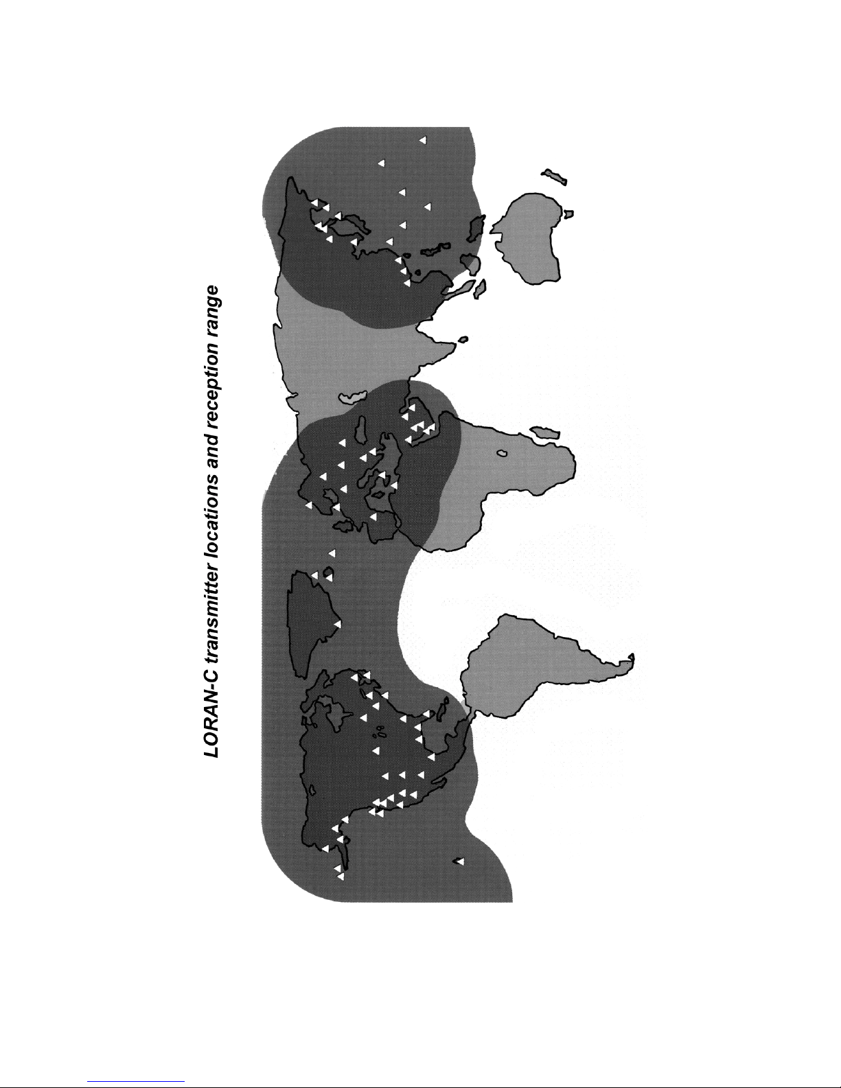
LORAN-C Station List 5
FS700 Overview 9
Introduction 9
Antenna 9
Signal Acquisition 9
Locking to LORAN-C 10
Signal Errors 10
Front/Rear Panel Features 11
Front Panel Features 11
Rear Panel Features 12
Front Panel Operation 14
Introduction 14
LORAN Tracking
Overview 14
Tracking Menu 15
GRI Selection 15
Station Selection 15
Search Mode 16
Time Constant 16
Keyboard Lock 16
Status Menu 17
Gain, Signal to Noise 17
Phase 17
Stations Fo und 18
Status Timing 18
Signal Quality 18
14
Tracking P o int M o nito ring 18
Notch Filters 19
Tuning the Notch Filters 19
Search Problems 20
Tracking Problems 21
Frequency Generation
and Calibration 23
Frequency Menu 23
Phase Menu 23
Time Menu 25
Setup Menu 25
Programming
Programming the FS700 27
Communications 27
GPIB Communication 27
Front Panel LED's 27
Data Window 27
Command Syntax 27
Programming Errors 28
Detailed Command List 28
Tracking Co ntrol Co mmands 28
Tracking S tatus Co mmands 30
Phase Meter Commands 31
Status Reporting Commands 33
Hardware Test Commands 34
Status Byte Definitions 35
Status Reporting 35
Serial Poll Status Byte 35
Standard Event Status Byte 35
LORAN Status Byte 36
Programming Examples 37
Microsoft C - Example 1 37
IBM Basic - Example 2 39
Test and Calibr ation
Troubleshooting 41
Self Test Errors 41
GPIB Interface Problems 42
Hardware Troubleshooting 43
16-Bit DAC Test 43
RF Circuitry Test 43
Integrator Test 44
i
Page 4

Peak Detector Test 44
Performance Tests 45
Introduction 45
Necessary Equipment 45
Tests 45
Start Tests 45
Front Panel Test 45
RF Bandwidth Test 46
Internal Self-Tests 46
Notch-Filter Check 47
10 MHz Oscillator Check 47
Phasemeter Check 48
FS700 Performance Test
Record - Scorecard 49
Calibration 50
Necessary Equipment 50
Coarse Oscillator Adjustment 50
Bandpass Filter Alignment 51
Notch Filter Alignment 53
FS700 Circuitry
Circuit Description 55
Front End/ Notch Filters 55
LORAN Front End 55
Microprocessor System 56
I/O Ports and Interrupt Driver 57
Gated Integrators 57
Gated Integrator Pattern RAM 57
A/D, D/A Converters 58
Clocks and Clock Outputs 58
Phase Comparators/Frequency
Output 59
Front Panel LED's/Switches 59
Unregulated Power Supplies 59
Power Supply Regulators 60
Active Antenna 60
Typical Specifications 75
Operation 76
Trouble Shooting 76
Calibration 76
Circuit Description 76
Line Voltage Selection 76
Line Fuse 76
FS710 Component Parts List 77
PC Layout 80
Schematic 81
Component Placement on PCB
Schematic Circuit Diagrams
Front End/Notch Filters 1/14
LORAN Front End 2/14
Microprocessor System 3/14
I/O Ports and Interrupt Driver 4/14
Gated Integrators 5/14
Gated Integrator Pattern RAM 6/14
A/D, D/A Converters 7/14
Clocks and Clock Outputs 8/14
Phase Comparator/Frequency
Output 9/14
Front Panel LED's/Switches 10/14
Unregulated Power Supplies 11/14
Power Supply Regulators 12/14
Spare IC's 13/14
Active Antenna 14/14
FS700 Component Parts List 61
FS710 Am plifier
FS710 – 10 MHz AGC Distribution
Amplifier
Introduction 75
Front Panel - Figure 1 75
ii
Page 5

SAFETY AND PREPARATI ON FOR USE
WARNING: Dangerous voltages, capable of causing death, are present in this instrument. Use
extreme caution whenever the instrument covers are removed.
WARNING: Watch for overhead power lines when installing the FS700's antenna. Contact with power
lines can be fatal.
This instrument may be damaged if
operated with the LINE VOLTAGE
SELECTOR set for the wrong AC line
voltage or if the wrong fuse is installed.
Line Voltage Selection
The FS700 operates from a 100 V, 120 V,
220 V, or 240 V nominal AC power source
having a line frequency of 50 or 60 Hz.
Before connecting the power cord to a power
source, verify that the LINE VOLTAGE
SELECTOR card, located in the rear panel
fuse holder, is set so that the correct AC
input voltage value is visible.
Conversion to other AC input voltages
requires a change in the fuse holder voltage
card position and fuse value. Disconnect the
power cord, open the fuse holder cover door
and rotate the fuse-pull lever to remove the
fuse. Remove the small printed circuit board
and select the operating voltage by orienting
the printed circuit board to position the
desired voltage to be visible when pushed
firmly into its slot. Rotate the fuse-pull lever
back into its normal position and insert the
correct fuse into the fuse holder.
Line Cord
The FS700 has a detachable, three-wire power
cord for connection to the power source and to a
protective ground. The exposed metal parts of
the instrument are connected to the outlet ground
to protect against electrical shock. Always use an
outlet which has a properly connected protective
ground.
Antenna
The FS700's vertical antenna should be installed
on the roof of a building. Watch for power lines
when installing the antenna.
Furnished Accessories
- Power Cord
- Operating Manual
Environmental Conditi ons
OPERATING
Temperature: +10° C to +40° C
(Specifications apply over +18° C to +28° C)
Relative Humidity: <90% Non-condensing
Line Fuse
Verify that the correct line fuse is installed
before connecting the line cord. For 100
V/120 V, use an 1 Amp fuse and for 220
V/240 V, use a 1/2 Amp fuse.
NON-OPERATING
Temperature:-25° C to +65° C
Humidity: <95% Non-condensing
iii
Page 6
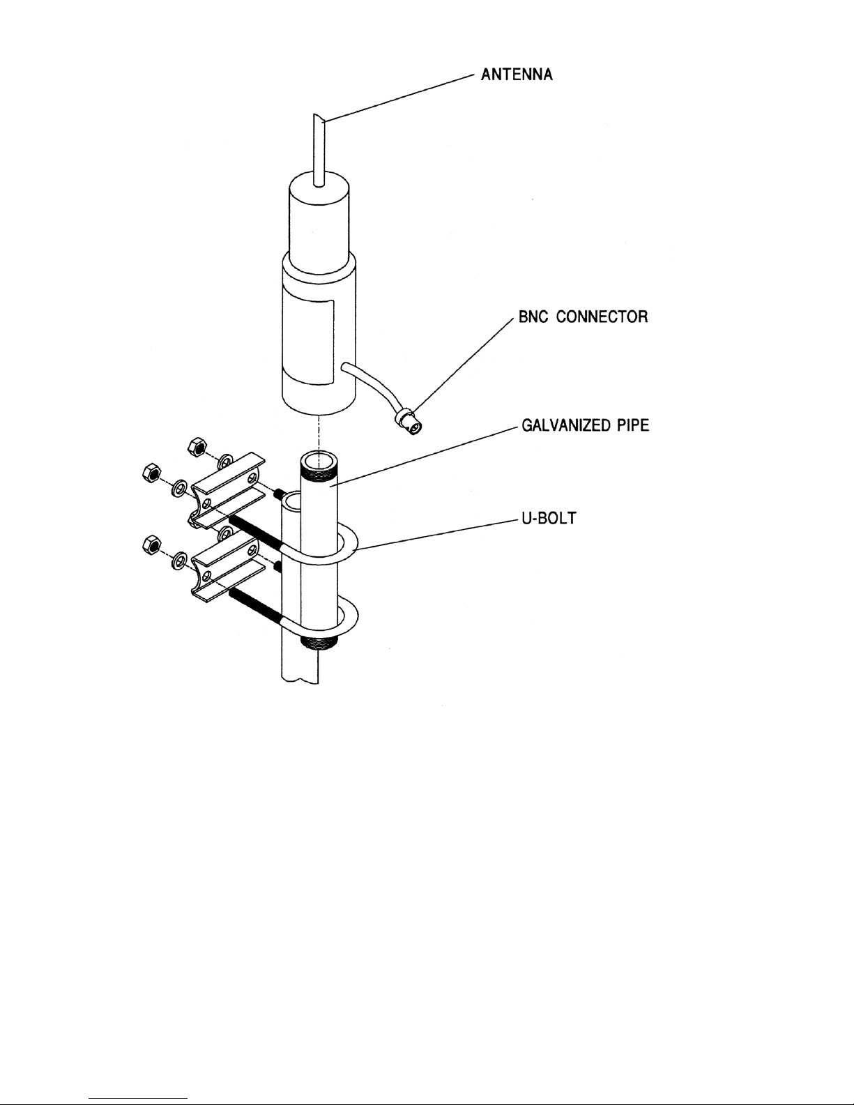
FS700 Antenna Installation Instru ctions:
New FS700 Antenna Installation Instructions:
The new style PVC base LORAN-C antenna used with the FS700 LORAN Receiver comes with a 6"
galvanized pipe nipple and 2 U-bolt clamps for mounting. After securing galvanized pipe with U-bolts,
the antenna base can be screwed onto the pipe nipple and the BNC connector can be connected to
the lead-in cable. The piece of supplied special heat shrink tubing should be applied over the cable
connection and heated with a heat gun or other heat source to weatherproof the connection.
The new antenna does not have an internal attenuator as with the old style antennas. If excessive
signal strength is encountered, consult the factory.
!!NOTE ON GROUNDI NG AND L IGHTNING PROTECTION!!
All metal antenna attachments should always be connected to a good earth ground. In areas where
lightning is encountered, a lightning arrester(s) should be used in the antenna lead-in cable.
iv
Page 7
v
Page 8

SPECIFICAT IONS
Receiver Specifications
Sensitivity Will lock with signal-to-atmospheric noise level of -10 dB or better.
LORAN Output Filtered and gain controlled antenna signal, typically 6 V peak-to-peak.
Station Search All available stations pre-programmed. Auto-Seek finds and tracks
strongest station.
Notch Filters 6 adjustable 30 dB notch filters, 3 at 40 - 90 kHz, 3 at 110 - 220 kHz.
Antenna 8 Foot Active Whip with 30 dB switchable attenuator, bandpass filter,
and FET preamp in weatherproof housing.
Freq uency Specif ications
Frequency Stability
Long Term 10
Short Term 10
10 MHz Outputs 4 outputs, 1 Volt peak-to-peak sine wave into 50 W.
Internal Oscillator
Standard Option/01
Frequency 10.000 MHz 10.000 MHz
Type AT Cut Ovenized SC Cut Ovenized
Aging 5 x 10
Allan Variance (1 s) 5 x 10
Stability 0-50° C 0.005 ppm 0.005 ppm
Phase Noise (dBc) -120 dBc, 10 Hz offset from carrier
-12
, the same as LORAN-C transmitter Cesium clock.
-10
, standard oscillator.
-11
10
, low phase noise option.
-10
per day 5 x 10
-11
-10
per day
-12
5 x 10
-155 dBc, 100 Hz offset from carrier
-165 dBc, 1 kHz offset from carrier
Phasemet er S pecificati ons
Frequency Output 0.01 Hz to 10 MHz in 1, 2.5, 5 sequence, TTL level.
Can be 50 Ω terminated.
Oscillator Input 1 kΩ, 0.5 V peak-to-peak minimum level. 50 Volts max.
vi
Page 9

Phase Output 0.01 V/degree, 0 to ±360°. Output proportional to phase difference
between OSC IN and FREQUENCY OUTPUT for frequencies between
100 kHz and 10 MHz.
Phase Resolution 3°
Interface
GPIB IEEE - 488 compatible interface. All instrument functions may be
controlled.
General
Operating 0 to 50° C.
Power 100, 120, 220 or 240 VAC +5% - 10%, 50/60 Hz, 50 Watts.
Dimensions 17" x 17" x 3.5". Rack mounting hardware included.
Weight 14 lbs.
vii
Page 10

ABRI DGED COMMAND LIST
Commands which may be queried have a ? in parentheses (?) after the mnemonic. The ( ) are not
sent. Commands that may only be queried have a '?' after the mnemonic. Commands which may
not be queried have no '?'. Optional parameters are enclosed by {}. i and j are integers.
Tracki ng Co ntrol Commands
AUTO(?) {i} Sets the search mode to AUTO (i = 1) or Manual (i = 0).
FLLT(?) {i} Sets the receiver time constant.
GRIP(?) {i} Sets the GRI to i micro seconds.
STOP Stops LORAN station tracking.
STRT Starts station acquisition.
STTN(?) {i} Sets the station to be tracked.
Tracki ng St at us Commands
GAIN? Returns the current receiver gain.
INFO? i Returns station search information.
LFOS? Returns instantaneous frequency correction.
LPHA? Returns current phase of internal clock relative to LORAN-C signal.
LSTA? Returns the index of the station being tracked.
NSTA? Returns the number of stations found during search.
STON? Returns the noise margin of the station being tracked.
TIME(?) {h,m,s} Sets/reads the time of day.
TLCK? Returns the amount of time the FS700 has been locked.
TULK? Returns the length of the last unlock period.
Phasemet er Command s
DLTF? Returns the frequency offset between the FREQUENCY OUTPUT and the
OSC IN BNC's.
FREQ(?) {i} Sets the frequency of the FREQUENCY OUTPUT.
PHSE? Returns the phase difference between the FREQUENCY OUTPUT and the
OSC IN BNC.
Status Reporting Commands
*CLS Clears all status registers.
*ESE(?) j Sets/reads the standard status byte enable register.
*ESR? {j} Reads the standard status register, or just bit j of register.
*IDN? Returns the device identification .
*PSC(?) j Sets the power on status clear bit. This allows SRQ's on power up if desired.
*RST Clears instrument to default settings.
*SRE(?) j Sets/reads the serial poll enable register.
*STB? {j} Reads the serial poll register, or just bit n of register.
SENA (?) j Sets/reads the LORAN status enable register.
viii
Page 11

STAT? {j} Reads the LORAN status register, or just bit n of register.
Hardw are Test Commands
(NOTE: These commands are not needed during normal operation.)
*TST? Starts self-test and returns status when done.
$ASC i Sets antenna input source. i = 0 = antenna, i = 1 = cal.
$DAT? Reads In phase and Quadrature gate data.
$GAT i Sets test gate patterns.
$INT? i Reads integrator data.
$POS i Sets gate position.
ATTN i Sets the attenuators to value i.
OSCF(?) i Sets the oscillator DAC to i.
ix
Page 12

QUICK ST ART INSTURCTIONS
When Installing the FS700 for the first time, it i s recommended that th e followin g procedure be
carried out. If a problem is encountered, please read the detailed discussion on instrument
operati o n (pages 1-46).
1) Make sure that the correct line voltage has been selected on the rear panel power entry module.
2) Install the antenna according to the instructions on pages iv and 9 of this manual.
3) While holding the BSP key down, turn the front panel power switch of the FS700 to the ON
position. After a second or two, release the BSP key. This procedure will initialize all data in the
FS700’s RAM. Notice that the OVEN LED in the STATUS section is on. It will take 20 minutes
for the internal 10 MHz oscillator to stabilize. At that point, the OVEN LED will turn off. (It is not
necessary to wait for the OVEN LED to turn off before proceeding.)
4) Press the TRACKING menu button on the front panel. Using the FIELD button, position the
cursor the GRI field and type in the appropriate GRI for your area. (Note that the GRI can also
be selected by scanning the LOCATION field. This is done by using the ARROW keys.)
5) Now you must wait until the OVEN LED goes off (approximately 20 minutes). When the OVEN
LED goes off, the SEARCH LED will immediately turn on and the FS700 will start acquiring the
LORAN signal. The search process will take between 15 and 40 minutes. After the FS700 has
successfully locked to the LORAN signal, the LOCK LED will turn on. Now the FS700 is ready
for operation.
x
Page 13
INT RODUCTION TO LORAN-C
LORAN-C is an accurate navigation system that is maintained by the
U.S. Coast Guard (LORAN stands for Long Range Navigation). A
receiver that measures the arrival times of the signals from three
LORAN stations can determine its position with an accuracy of about
1000 feet at a range of over 1000 miles. Because of the desire for
good long range position accuracy, the frequency and transmission
time of each LORAN transmitter is controlled by a set of Cesium clocks
or Hydrogen masers whose frequency accuracy is maintained by the
U.S. Naval Observatory. Because the timing characteristics of the
LORAN transmission are so tightly controlled, a receiver measuring the
signal from a single LORAN station can produce a very accurate
frequency output that is traceable to the U.S. Naval Observatory and
NIST. LORAN-C transmissions are also highly reliable. The stations
are functional more than 99% of the time and signal errors usually last
only a f ew minutes.
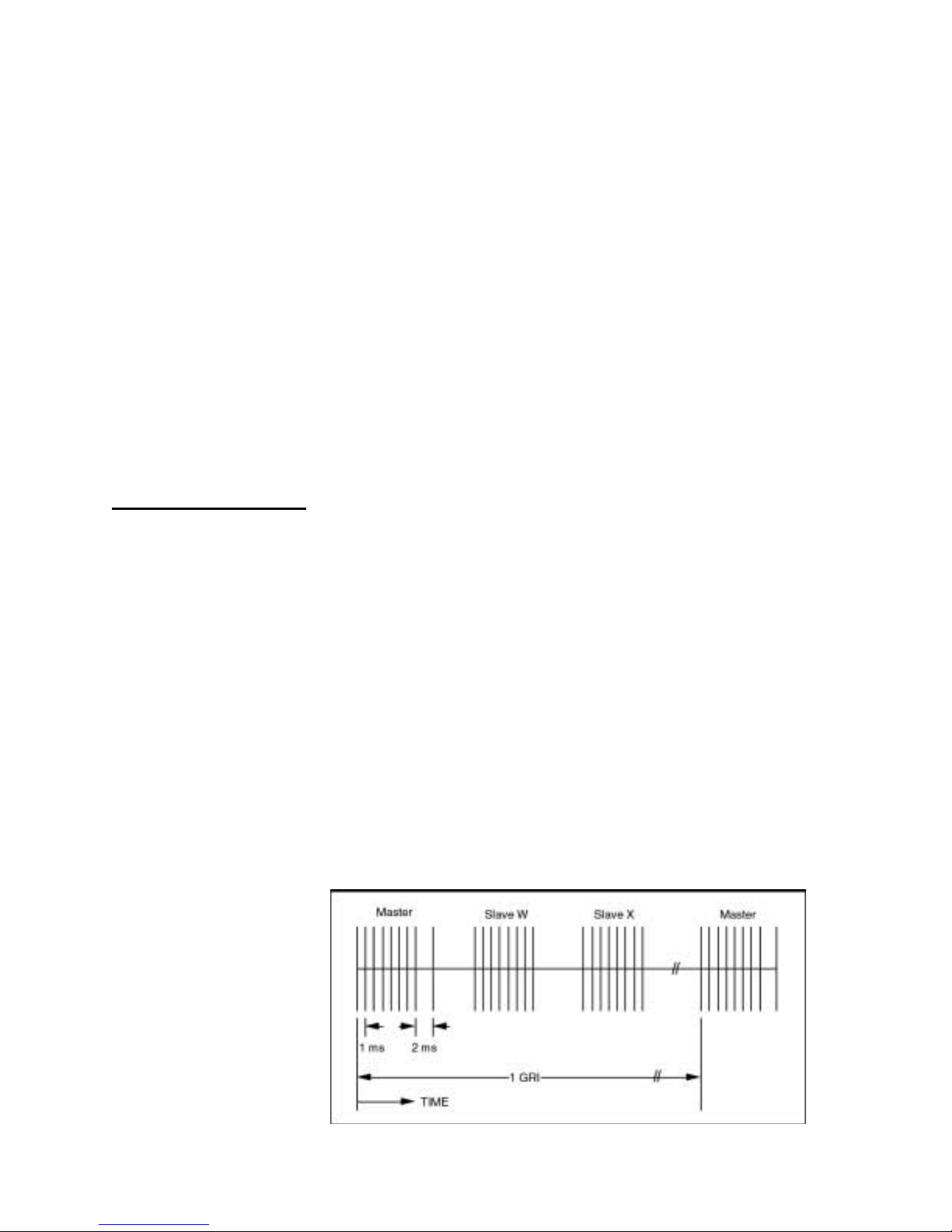
Signal Characterist ics
Signal LORAN-C stations transmit a pulsed signal at a carrier
frequency of 100 kHz. This frequency was chosen for stable
propagation characteristics and low ground wave attenuation. The
transmissions of the various stations are differentiated by the timing of
their pulses. The LORAN transmitters in a specific geographical region
are arranged in groups of at least three (the minimum number needed to
establish position) to at most 6 stations called chains. The chains are
differentiated by the repetition rate of the pulses transmitted by the
stations in the chain. This rate is called the Group Repetition Interval, or
GRI. For example, the U.S. West Coast chain has a GRI of 99400 µs
and each station in that chain (4) will transmit its signal once every
99400 µs. If the receiver synchronizes its timing with the desired GRI,
only stations in that GRI will produce a stable signal. Each chain has a
master station (labelled "M") and up to four secondary stations
(labelled "V", "W", "X", "Y", and "Z"). Once every GRI, each station will
transmit a group of eight pulses at the 100 kHz carrier frequency. Each
pulse is about 250 µs long, and the pulses are separated by exactly 1
ms. The master station has a ninth pulse that is transmitted 2 ms after
the eighth pulse. This ninth pulse identifies the station as the master.
The master station always transmits first in the GRI followed by each
Figure 1
Transmission of LORAN
Signals During a GRI
1
Page 14
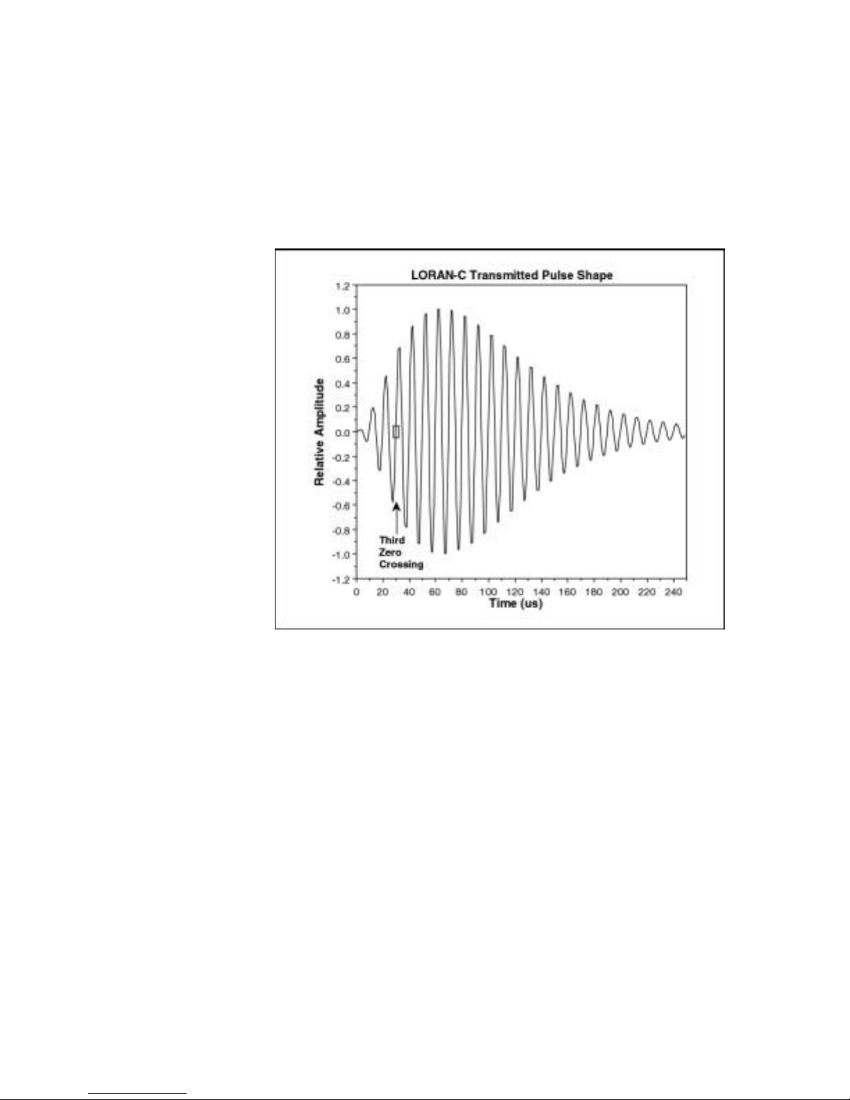
Graph 1
Shape of the Transmitted
LORAN-C Pulse
secondary station in a prescribed order. The signals are transmitted so
that the pulse groups will never overlap within the reception range of the
stations. This is shown in Figure 1. The receiver determines its
position from the time differences between the transmissions from each
station, and the known positions of the transmitters. If the master
station cannot be received, there is no way to identify the stations and
also no way to determine the receiver's position.
The Coast Guard controls the accuracy of the LORAN-C system by
precisely controlling the transmitter carrier frequency and the pulse
emission time. The pulse emission time is controlled by accurately
setting the emission time of the third positive zero crossing of the
LORAN rf pulse. This point is called the PULSE TIME REFERENCE
(PTR), and was chosen as a compromise between adequate signal-tonoise ratio and freedom from skywave interference (discussed below).
The shape of the LORAN pulse is shown in Graph 1. By carefully
tracking the PTR over long time intervals it is possible to extract the
inherent frequency accuracy of the LORAN transmitter's Cesium clock.
This is the function of the FS700 LORAN-C Frequency Standard. The
FS700 will produce a frequency output with the same long-term
accuracy as a USNO controlled Cesium clock as long as a single
station in any GRI is receivable.
2
Page 15

Phase Codi ng
LORAN transmissions are Phase Coded to minimize the effects of
random noise, CW signal interference, and skywave interference.
Some of the pulses in the eight pulse group are transmitted with the
carrier signal inverted with respect to the rest of the pulses. That is,
some pulses are transmitted with the first cycle of the pulse starting by
going negative instead of positive. The phase code repeats in a two
GRI period called a Frame. A receiver, such as the FS700, that takes
phase coding into account will cancel any interference that occurs on an
interval longer than a frame. Also, the phase coding is arranged so that
any long delayed skywave interference will also be cancelled. The two
GRI pulse groups within a frame are called Group A and Group B and
have different phase codings. Additionally, master station frames have
a different phase coding than secondary station frames. The phase
codings for the various frames are shown in Figure 2.
Figure 2
Phase Codings of Master
And Secondary Stations
Signal Propagation
Group Master Secondary
A ++--+-+- + +++++--+
B +--+++++ - +-+-++--
The transmitted signal from a LORAN transmitter is split into two parts:
the groundwave which travels parallel to the surface of the earth, and
the skywave, which travels upward through the atmosphere, is reflected
by the ionosphere, and returns to earth. Because the height of the
ionosphere depends on the time of day, the season, and solar activity,
the skywave propagation path and the propagation delay are very
unstable. This makes the skywave transmission less than ideal for
accurate timing. The groundwave transmission does not suffer these
problems and is a very stable source of timing information. However,
the groundwave signal is rapidly attenuated by the atmosphere and
suffers contamination from the skywave signal which arrives slightly
later in time. These considerations limit the groundwave reception
range of the LORAN signal to about 1500 miles. At this range the
skywave interference will never disturb the position of the PTR.
Bli nk Tran smissions
Additional Information
Occasionally a LORAN transmitter will malfunction so that its
transmitted signal is no longer accurate. When this occurs the master
station and the affected secondary station begin blink transmissions.
The master station will blink its ninth pulse in a coded pattern indicating
which secondary is bad, while the secondary station will blink its first
two pulses in 0.25 seconds on, 3.75 seconds off pattern. The other
pulses in the transmission are unaffected. By checking for blink the
FS700 is able to ensure that it is locked to a healthy transmitting station.
More detailed information may be obtained from:
3
Page 16

1) United States Naval Observatory, Time Services Division
34 Massachusetts Ave.
Washington, DC 20390
(202) 653-1507
Ask to be placed on the LORAN-C chain information mailing list.
LORAN-C station propagation delays may also be obtained from:
2) United States Coast Guard Headquarters
Washington, D.C. 20593
(202) 267-0283
The LORAN-C specifications may be obtained.
Publication numbers:
LORAN C User Handbook COMDTINST M16562.3
Specification of the LORAN C Transmitted Signal COMDTINST
M16562.4
4
Page 17

X Fox Harbor, Labrador, Canada
Chain GRI Station Transmitter Location
Newfoundland East 72700 µs M Comfort Cove, Canada
Coast W Cape Race, Canada
W Jan Mayen, Norway
X Berlevag, Norway
W Jan Mayen, Norway
Bo 70010 µs M Bo, Norway
Ejde 90070 µs M Ejde, Faeroe Island, Denmark
X Bo, Norway
Y Vaerlandet, Norway
Z Loop Head, Ireland
X Soustons, France
Lessay 67310 µs M Lessay, France
Y Loop Head, Ireland
Z Sylt, Germany
X Lessay, France
Y Vaerlandet, Norway
Sylt 74990 µs M Sylt, Germany
French SNR 89400 µs M Lessay, France
X Soustons, France
X Lampedusa, Italy
Z Estartit, Spain
Mediterranean Sea 79900 µs M Sellia Marina, Italy
V Salwa, SA
Saudi Arabia North 70300 µs M Afif, SA
W Al Khamasin, SA
X Ash Shaykh Humayd, SA
Z Al Muwassam, SA
W Salwa, SA
X Afif, SA
Saudi Arabia South 88300 µs M Al Khamasin, SA
Y AshShaykh Humayd, SA
Z Al Muwassam, SA
X Shoal Cove, Alaska, USA
Y George, Washington, USA
Z Port Hardy, BC, Canada
Chain GRI Station Transmitter Location
West Coast USA 99400 µs M Fallon, Nevada, USA
W George, Washington, USA
X Middletown, California, USA
Y Searchlight, Nevada, USA
Canadian West Coast 59900 µs M Williams Lake, BC, Canada
North Central USA 82900 ms M Havre, Montana, USA
W Baudette, Minnesota, USA
X Gillette, Wyoming, USA
Y Williams Lake, BC, Canada
V Gillette, Wyoming, USA
W Searchlight, Nevada, USA
X Las Cruces, New Mexico, USA
Y Raymondville, Texas, USA
Z Grangeville, Louisiana, USA
South Central USA 96100 ms M Boise City, Oklahoma, USA
W Malone, Florida, USA
X Seneca, New York, USA
Y Baudette, Minnesota, USA
Z Boise City, Oklahoma, USA
Great Lakes 89700 µs M Dana, Indiana, USA
5
W Grangeville, Louisiana, USA
X Raymondville, Texas, USA
Y Jupiter, Florida, USA
Z Carolina Beach, NC, USA
W Caribou, Maine, USA
X Nantucket, Massachussetts, USA
Southeast USA 79800 µs M Malone, Florida, USA
Northeast USA 99600 µs M Seneca, New York, USA
Y Carolina Beach, NC, USA
Z Dana, Indiana, USA
Y Cape Race, Canada
Z Fox Harbor, Labrador, Canada
X Nantucket, Mass., USA
Canadian East Coast 59300 µs M Caribou, Maine, USA
Page 18

X Raoping, PRC
6
Y Rongcheng, PRC
67300 µs X Raoping, PRC
Y Chongzuo, PRC
W Veraval, India
X Billamora, India
W Diamond Harbour, India
4/1/9
X Patpur, India
Chain GRI Station Transmitter Location
China East Sea 83900 µs M Xuancheng, PRC
W Petrozvodsk, Russia
China South Sea** 67800 µs M Hexian, PRC
X Solnim, Russia
Y Simferopol, Ukraine
Z Syzran, Russia
Bombay 60420 µs M Dhrangadhr, India
Calcutta 55430 µs M Balasore, India
W Petropavlo, Russia
X Ussuriisk, Russia
Y Kurilsk, Russia\
Z Ohotosk, Russia
** Broadcasting on two diferent GRI
W Kwang-Ju, Korea
X Gesashi, Okinawa
Y Niijima, Japan
Z Ussuriisk, Russia
W Gesashi, Okinawa, Japan
X Marcus Island, Japan
Y Tokatibutto, Hokkaido, Japan
Z Pohang, Korea
X Attu, Alaska, USA
Y Aleksandrovsk, Russia
USA
X Attu Alaska, USA
Y Point Clarence, Alaska, USA
Z Narrow Cape, Alaska, USA
X Narrow Cape, Alaska, USA
Y Shoal Cove, Alaska, USA
Z Port Clarence, Alaska, USA
X Xuancheng, PRC
Y Helong, PRC
Chain GRI Station Transmitter Location
Western Russia 80000 µs M Bryansk, Russia
Eastern Russia 79500 µs M Aleksandrovsk, Russia
East Asian 99300 µs M Pohang, Korea
Northwest Pacific 89300 µs M Niijima, Japan
6
Russian –American 59800 µs M Petropavlo, Russia
North Pacific 99900 µs M Saint Paul, Pribilof Is., Alaska,
Gulf of Alaska 79600 µs M Tok, Alaska, USA
China North Sea 74300 µs M Rongcheng, PRC
Page 19

7
Page 20
8
Page 21

FS700 OVERVIEW
Introduction
Antenna
The FS700 LORAN-C Frequency Standard produces a highly stable
and accurate 10 MHz output by locking an internal crystal oscillator to
the Cesium clock controlled LORAN-C radio transmission. The FS700
system consists of a receiver, containing amplifiers, filters, and data
acquisition circuitry, and a remote antenna, with an internal preamplifier.
Data acquisition circuitry allows the FS700 to frequency lock its internal
oscillator to the third positive zero crossing of the LORAN-C
transmission. In addition to providing an ultra-stable 10 MHz output, the
FS700 also provides a user selectable TTL compatible frequency
output in the range of 0.01 Hz to 10 MHz in a 1, 2.5, 5 sequence. An
internal phasemeter circuit allows precise frequency calibrations of
other oscillators in the range of 100 kHz to 10 MHz.
The FS700 should be used with the supplied antenna. Do not use
another antenna because the antenna box contains filter and amplifier
circuits that are necessary to the FS700. Mount the antenna outside,
vertically, and preferably on the roof of a building. Connect the antenna
to the FS700 with shielded cable up to 1000 feet long. Use either 50 or
75 ohm cable, since the impedance of the cable is not critical. A 100
foot, 50 ohm cable is supplied with the FS700.
Signal Acquisition
After the user chooses and enters the desired GRI, the FS700 will
acquire the LORAN-C signal (the SEARCH LED will turn on). First,
automatic gain control (AGC) software adjusts the receiver gain so that
the signal at all points in the GRI is at full scale (about 6 V pk-pk at the
LORAN OUT connector). Next, the entire GRI is searched for the
presence of LORAN pulses. After the pulses are found, and the
stations identified, the desired station is chosen. This station may be
selected automatically to be the largest signal detected, or the user may
enter a specific station of choice. After the station is chosen the
receiver identifies and matches the phase coding of the selected
station.
The FS700 then begins to frequency lock to the entire pulse envelope
of the selected station. This initial frequency locking removes any initial
-7
gross frequency offset (up to 2 x 10
) and allows more time for the
determination of the third zero crossing position. When the frequency
-9
offset has been reduced to better than 1 x 10
, the phase offset
between the internal oscillator and the LORAN signal is set to zero and
the frequency lock is terminated. The FS700 then identifies the location
of the third zero crossing of the LORAN pulse. After the third zero
crossing has been located, the frequency lock is restarted to lock to the
third zero crossing position. At this point the FS700 enters lock mode
(the LOCK LED will turn on) and begins tracking the third zero crossing.
9
Page 22

The entire search process takes between 15 and 40 minutes depending
on the signal-to-noise ratio of the station selected.
It is important to understand that at large distances (>1000 miles) from
the LORAN transmitter, the LORAN skywave signal can be many times
larger than the groundwave signal. The FS700 can detect and correctly
handle this condition until the skywave is abo ut 5 times the gro undwave
amplitude. At this point, the FS700 will most likely lock to the skywave.
This results in poor long term stability because of the diurnal shifts in
the skywave timing. If this occurs, a different station should be chosen.
Lo cking t o LORAN-C
Signal E rrors
Once in LOCK the FS700 keeps the frequency difference between the
internal oscillator and the LORAN transmission at a minimum. This is
accomplished by using a software frequency-locked loop (FLL). The
frequency-locked loop adjusts the internal oscillator's frequency so that
the frequency difference at all times is zero. This is different than a
phase-locked loop (PLL). A PLL attempts to always keep the phase
difference at zero, and may introduce a large instantaneous frequency
offset to change the phase. Thus, a FLL will have better phase noise
and short-term stability than a PLL. The time constant of the FS700's
FLL is set according to the signal-to-noise ratio of the signal, and is
generally about 2000- 5000 GRI. The FS700 also has an auxiliary PLL
that keeps the phase difference between the FS700 and the LORAN
signal small. The time constant for the PLL is much longer than the FLL
time constant, and has no effect on short-term stability (the frequency
offset due to the PLL averages to zero and is rarely instantaneously
-11
larger than 1-2 x 10
).
During locking, the FS700 monitors the received signal and checks for
error conditions. If an error is detected, the FS700 will halt its FLL (to
prevent erroneous frequency adjustments) and wait. If the error
condition goes away within 20 minutes, the FLL will restart and will
continue as before. If the error does not go away, one of two things
may happen. If the search mode is set to manual, the FS700 will
terminate its lock. If the search mode is set to auto, the FS700 will
attempt to reacquire a station. If the station selection is set to a
specific station (not auto station selection), the FS700 will continue to
try to acquire the station selected until the station returns to health.
10
Page 23

FRONT / REAR PANEL FEATURES
Front Panel Features
1) Power Switch Pressing the power switch turns the FS700 on and off. In STBY
position only, the ovenized oscillator is on. This minimizes warm-up
time.
2) Numeric Keypad The numeric keypad allows entry and modification of parameters in the
FS700's menus. Data can be entered in two modes depending on the
menu item displayed. In numeric mode (NUM LED on), data is entered
as a number with the keypad. The entry is terminated using the execute
(EXC) key. Typographical errors may be corrected using the
backspace (BSP) key. Pressing BSP with no number displayed will
cause the FS700 to return to the previous value. In cursor mode (<>
LED on) a menu item is modified pressing the up and down arrow keys
(8 and 2). If neither the NUM or <> LED's are lit, then the selected item
may not be modified.
3) Field Key In many menus, several selections are displayed. A flashing cursor
denotes the modifiable item. Pressing the FIELD key causes the cursor
to cycle through the available choices. If the FS700 is in GPIB remote
mode, pressing the FIELD key returns the unit to local mode.
4) Menu Keys The menu keys co ntrol which menu is displayed. Several menus have
more than one screen of data. The various screens of data may be
displayed by repeatedly pressing the associated menu key.
5) Status LED's The 5 status LED’s indicate the current status of the FS700.
LED Meaning
LOCK The FS700 locks to and tracks a station.
SEARCH The FS700 searches for a station.
ERROR An error has been detected. A relevant error message
will also be displayed. These errors can be signal
errors, command programming errors, etc.
OVEN The oven LED is on at power-up which indicates the
internal oven may be cold. The LED stays on for 20
minutes, and AUTO station search does not begin until
this warm-up period is over. This LED is lit when the
oscillato r uses up mo re than 75% o f its tuning range,
(about ±3 Hz).
ANT This LED indicates the antenna is faulty.
6) LCD Display The 32 character by 2 line LCD display shows menu items and
informational messages. If the displayed message is not a menu item,
11
Page 24

it is either an error or an informational message. To retrieve the menu
display, just press any key.
7) LORAN Output This BNC outputs the amplified and filtered antenna signal. This may
be used in conjunction with the rear panel GRI SYNC and GATE
outputs to view the receiver's tracking point. The output is about 6 V
pk-pk and will drive a high impedance load.
8) Frequency Output This connector can be set to output a TTL level signal (2.5 V into 50
ohms) at a frequency between 0.01 Hz and 10 MHz in a 1, 2.5, 5
sequence. This output may be terminated into 50 ohms.
9) Oscillator Input This is the input to the FS700's internal phasemeter. The input signal to
the phasemeter should have the same frequency as the FREQUENCY
OUTPUT. The input has a 1 kohm input impedance and requires a
signal level of about 300 mV pk-pk. This input is protected to 100 VDC
and 40 VAC.
10) Phase Output This is the phasemeter analog output. The output voltage is
proportional to the phase difference between the OSCILLATOR INPUT
and the FREQUENCY OUTPUT with a coefficient of proportionality of
0.01 V/degree. This output has a range of ±360 degrees (±3.6 V) and
expects a high impedance load.
Rear Panel Features
1) Power Entry Module The power entry module contains the FS700's fuse and the line voltage
selection card. Be sure that the fuse rating matches that listed on the
rear panel and that the line voltage is set to the local value. To set the
line voltage: remove the power cord, remove the fuse, remove the
voltage selector card from the power entry module, insert the voltage
selector card so that the desired line voltage is visible through the clear
plastic window, replace the fuse with a correct rated fuse for the line
voltage selected, and reconnect the power cord.
2) IEEE-488 Connector This connector can be used with any standard IEEE-488 (GPIB) cable
to allow computer control of the FS700.
3) GRI SYNCH Output These two outputs may be used in conjunction with the front panel
Gate Output LORAN OUTPUT to view the FS700's tracking point. Both outputs
provide TTL level outputs and may have a 50 ohm termination. The
GRI SYNC output provides a negative going pulse at the start of each
GRI. When the receiver is in LOCK (LOCK LED on) this pulse occurs
500 ±5 ms before the receiver tracking point, and the GATE output
brackets the third zero crossing point with a negative going pulse.
These outputs may be used with an averaging digital oscilloscope (such
as HP 54501A) to view the Loran pulse tracking point. This procedure
is detailed in the tracking section of this manual.
12
Page 25

4) 10 MHz Outputs These four outputs provide a 1 V pk-pk 10 MHz output when terminated
into 50 ohms. These outputs are individually buffered and are shortcircuit protected.
5) Lock Output This is a TTL compatible output that is high when the receiver is locked
(LOCK LED on). This output is a transistor with a 10 kohm pull-up
resistor. This output may be wire-or'd with other similar outputs as long
as the current sink capability is greater than 0.5 mA.
6) Antenna Input This is the connector for the remote antenna. The antenna cable may
be up to 1000 ft long. The FS700 must be used with the antenna that is
supplied.
7) RS232 Connector This connector is used for RS232 communication.
(Optional)
13
Page 26

FRONT PANEL OPERATION
Introduction
LORAN Tracking
The parameters controlling the operation of the FS700 are displayed
and adjusted in a set of six menus. Each menu may have one or more
screens (two line displays) of data. Each screen may contain one or
more field (adjustable parameter). Pressing a menu button displays that
menu. The screens that belong to a menu may be displayed by
repeatedly pressing the menu button. The field that is adjustable is
denoted by a flashing cursor bar. The various fields may be selected by
pressing the FIELD key.
The data entry mode for each field is indicated by the mode LEDs
above the field key. If the NUM LED is lit the data is entered in numeric
format using the keypad. Pressing the EXC key terminates the entry.
Errors are corrected using the backspace (BSP) key. If the <> LED is
lit the field is changed with the cursor keys (up and down arrow keys). If
neither LED is lit the display may not be changed.
Occasionally, an error or informational messages will be displayed on
the LCD display. The display may be returned to the normal menu
display by pressing any key.
The TRACKING and STATUS menus control the FS700's tracking of a
LORAN-C station. Adjustable tracking parameters are set in the
TRACKING menu, while tracking status is displayed in the STATUS
menu.
Overview Most of the FS700's operation is completely automatic. First, choose a
GRI and enter it into the FS700. Refer to the LORAN chain map to
choose a GRI that has stations near the receiver. Then, LORAN-C
station selection, acquisition, and tracking can begin. Station selection
and search mode may be either manually or automatically controlled.
Station selection is the process of choosing a specific station in the
GRI for tracking. In AUTO station selection, the FS700 will choose and
track the station with the largest signal strength. AUTO selection is the
FS700's default mode, and is recommended for general use. The
FS700 may be set to track a specific station in the GRI. If the master
station is not detected there is no way to identify the stations and
manual station selection will f ail. AUTO selection will pick the largest
signal even in the absence of the master.
The FS700's search mode controls the starting and stopping of
searches, and recovery from signal errors. In AUTO mode the FS700
will begin a search anytime that it is unlocked from a station. While in
MANUAL, the searches must be started by pressing the EXC key. The
FS700's default is AUTO. After power-on, an AUTO search will begin
after the oven oscillator warm-up period expires (the OVEN LED goes
off). A MANUAL search may be started at any time. However, if the
14
Page 27

oscillator is not fully warmed up the search may fail. When in AUTO, if
a signal error forces the FS700 to terminate locking, the FS700 will
automatically start a new search. While in MANUAL, a new search
must be started by pressing the EXC key.
GRI: 99400 µs Station: X
Location: Middletown, CA USA
Tracki ng Men u
GRI Selection The first field is the GRI to which the FS700 is to lock. Set the GRI to a
Station Selection Station selection is set with the second field. Adjust this setting with the
The first screen has three adjustable parameters and is used to set the
station that the FS700 is to track. If the FS700 is tracking a station,
changing any of these parameters will cause the FS700 to unlock. To
prevent accidental unlocks, a warning message requiring confirmation
of the change will be displayed.
value appropriate to the location of the receiver by referring to the
LORAN chain map to select the GRI for the nearest stations. The GRI
must be set to a value between 40000 and 99990 ms in steps of 10 ms.
up and down arrow keys. The default setting is "AUTO", and the
FS700 will automatically choose the station with the largest signal. The
FS700 may be be set to a specific station - "M" (master), or one of
secondaries. If a chain existed at the chosen GRI when the FS700 was
shipped, the actual station names (a subset of V, W,X,Y, and Z) will be
displayed; otherwise the secondary may be set to an index of A,B,C, D,
or E - the order of transmission of the secondaries. The identification
of the secondaries is determined by the timing of the secondaries
relative to the master station. For a chain not in the FS700's station list
a default set of times will be used- an average of the timings of existing
chains. If the unknown chain's timing differs greatly from typical it may
not be possible to identify and select a particular secondary. However,
the master may always be selected, and AUTO will always select the
largest station- regardless of the identification of the secondaries. This
allows the FS700 to be set to any possible LORAN station, even if it
didn't exist at the time of the FS700's production. Once a station has
been chosen, during AUTO station selection the FS700 will display the
station identification in parentheses after the word AUTO. For
example: AUTO (Y) if Y has been chosen. If the FS700 is set to lock to
a specific station and the master station is not found, the selected
station will not be identified and the search will fail.
The third field is the station location field. This field displays the location
(station name) of the selected station. By scrolling through this list
using the up and down arrow keys a station near the receiver may be
chosen. All stations that existed at the time of the FS700's production
are in this list. If no station exists at the current GRI or station choice
15
Page 28

the location message will display that fact. In AUTO station selection
the FS700 will display the station location once a station is chosen.
Search Mode: Auto
Start Station Acquisition (EXC)
Search Mode The second screen has two parameters and controls the starting and
stopping of the locking process. The first field controls the SEARCH
MODE. In AUTO search mode the FS700 will automatically begin a
station search any time it is unlocked. In MANUAL mode pressing EXC
will start the search. If a signal error occurs and the FS700 unlocks, the
FS700 will automatically reacquire a station in AUTO mode, while in
MANUAL the lock must be manually restarted. The second field
controls starting and stopping of locking and searches. If the FS700 is
not currently searching or locked, pushing the EXC button will start a
search. If the FS700 is searching or locking, pressing the EXC button
will stop the lock. In AUTO search mode, a new search will
automatically be started once the EXC button is pressed to stop the
search. If manual control is desired, the mode should be set to manual.
Receiver Time Constant: 4096 GRI
Time Constant The FS700's tracking time constant is set in the third screen in units of
GRI. The time constant is adjusted using the cursor keys, and can be
set between 128 and 16384 GRI. The time constant sets the amount of
signal averaging and the time between corrections of the FS700's
oscillator frequency. The setting is a trade-off between averaging
enough to reduce signal noise, and correcting frequently enough to
correct oscillator frequency changes with room temperature, etc.
Recommended settings are 2048 GRI with the standard oscillator, and
4096 GRI with option 1. If the signal-to-noise ratio of the station being
tracked is poor (< -3 dB), the time constants should be increased by a
factor of two or four. In general, there is no reason to reduce the time
co nstants below their nominal value.
Tracking Keys Lockout: On
Enter Password to Lock Keys:XXXXX
Keyboard Lock The menu items that control the FS700's station tracking may be locked
to prevent unauthorized modification. To lock all items in the
TRACKING and CAL menus, enter a password up to 4 digits long.
Entering the password again will unlock the menu items. On power-up
the keyboard lock is automatically cleared. Other features of the
FS700, such as the FREQUENCY OUTPUT and PHASE meter will
operate normally while the TRACKING menus are locked.
16
Page 29
Receiver Gain: 75dB
Noise Margin: 33dB
Status Menu
Gain, Signal to Noise The first screen displays the FS700's gain and signal-to-noise ratio.
The gain is the gain necessary to bring the selected station to full scale
signal level. The maximum value is 120 dB. Noise Margin indicates the
current LORAN signal quality. A noise margin of 0.0 db is the poorest
quality signal useable by the FS700. The maximum value is +55 dB.
The gain number is not displayed until after station selection, while the
noise margin is not calculated until after the third zero crossing is
located.
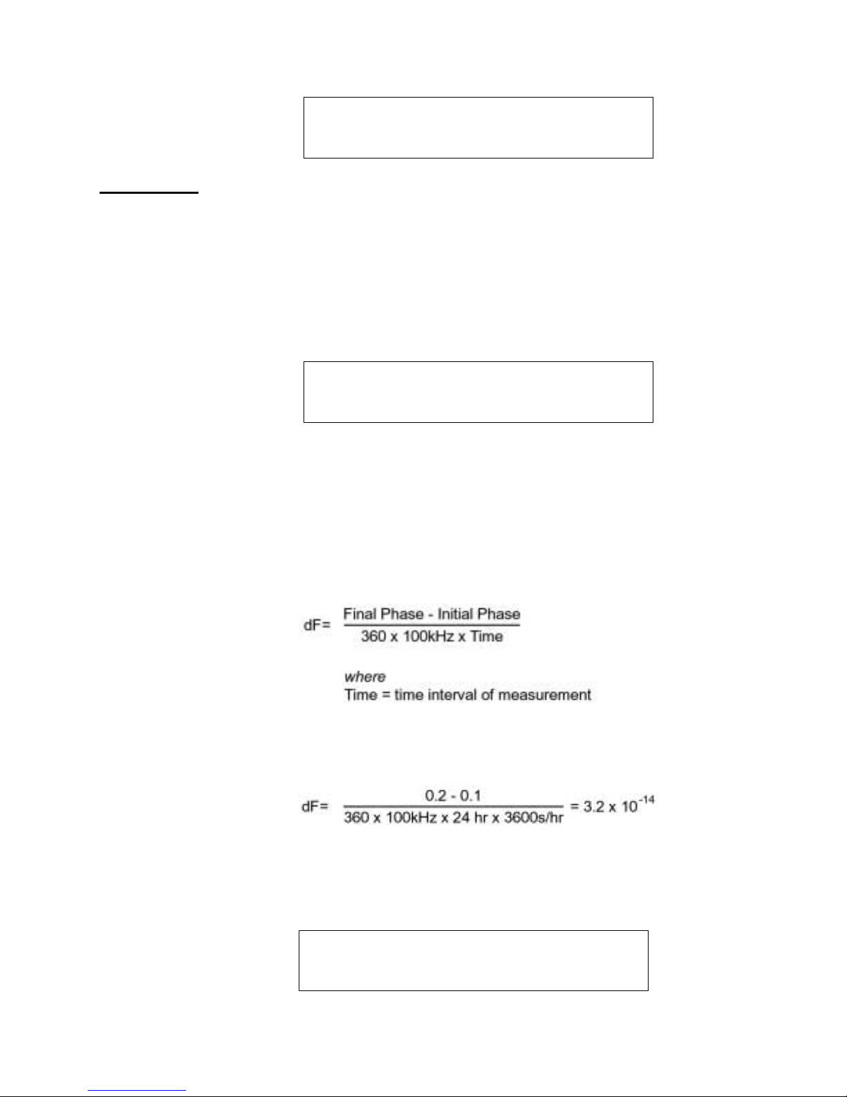
LORAN Frequency Offset: 2.0 E-11
Phase: 0.2°
Phase The second screen displays the instantaneous frequency offset of the
FS700's oscillator from the LORAN signal. That is, it is the value of the
last correction that the FS700 made to its oscillator. The time average
of this value is zero. The oscillator has a sensitivity of about 1 x 10
11
minimum step size. Also displayed is the instantaneous phase of the
FS700's sampling gate relative to the LORAN pulse (in degrees). The
long-term fractional frequency difference over any time interval may be
calculated from the f o llo wing f o rmula:
-
For example: Suppose at the start of a 24 hour period, the phase is 0.1
degree. While at the end of the time interval, the phase is 0.2 degree.
Then the average frequency difference is :
This means that over a 24 hour period the FS700's oscillator is every
bit as good as the source in the LORAN transmitter. The transmitter's
Cesium clock is accurate to about 1-2 x 10
period.
-12
over the same time
Stations Found (Ident: Amp in dB)
M57 V38 W45 X70* Y44
17
Page 30

Stations Found The third screen displays the identification and amplitude of all stations
found during the search phase of station acquisition. The amplitudes
are displayed in relative dB, and the station that the FS700 is locked to
has a "*" next to it. The station identifications will be displayed if the
FS700 knows them. If the master station is not found, the
identifications will be listed as "?". If there were no stations assigned at
the time of the FS700's manufacture the stations will be listed as "M",
"A","B", etc., since the station labels are unknown. This display is
useful in determining the number and strength of the stations in the
receiver's location.
Time Since Lock:12:34:56
Length Last Unlock: 0:00:00
Status Timing The fourth screen displays the amount of time that the FS700 has been
locked to its station. This timer can go up to 32767 hours (3.75
years)before it rolls over back to zero. Also displayed is the duration of
the most recent time at which the FS700 was unlocked. If the FS700
has never been unlocked this number will be 0:0:0. However, if the
FS700 ever became unlocked and had to reacquire a station, the length
of time until it became relocked will be displayed. These two times may
be used to determine when the FS700 became unlocked.
Signal Status: A r b n o
Press EXC to clear status
Signal Quality The last screen displays information on the quality of the received
signal and any transient conditions that may have occurred. The letters
a, r, b, n, and o indicate the status of antenna, rf, blink, noise margin,
and oscillator warnings. If the letter is displayed in lower case, the
condition has not occurred. If the letter is in UPPER case, the
condition has been detected in the past. When a warning condition is
detected, the associated status indicator is set. The indicators may be
reset by pressing EXC. Relocking the receiver will also reset the
indicators. The various warnings are described below in the
TRACKING PROBLEMS section.
Track Point Monitoring It is useful (or confidence building) to monitor the FS700's tracking point
(the third zero crossing). This is easily done using a digital oscilloscope
that is capable of averaging many signal traces (such as the HP
54501A). The averaging is necessary to reduce the noise on the signal.
While the FS700 is locked, the GRI SYNC output on the FS700's rear
panel provides a negative going pulse every GRI 500 ±5 µs before the
third zero crossing. The GATE output provides a negative going pulse
that brackets the third zero crossing. To monitor the tracking point,
trigger the scope with the GRI SYNC pulse. After the FS700 has
locked, display the LORAN OUTPUT and GATE output on the scope
using a 10 µs/div scale with 500 µs of trigger delay. This puts the gate
18
Page 31

pulse in the middle of the screen. Set the scope to average about 1000
triggers. After the signal has averaged for a while, the LORAN pulse
should be easily visible. By expanding the vertical scale it is easy to
see the start of the pulse. It is simple to observe the tracking point by
counting zero crossings and remembering that the LORAN pulse starts
with a positive half cycle that doesn't count as a zero crossing.
Notch Filters The FS700 has six adjustable notch filters that may be used to eliminate
strong interfering signals. Three of the filters can tune from 40 to 90
kHz while the other three tune from 110 to 220 kHz. The filters are
tuned by using the six rear panel screw adjustments. Because these
filters severely affect the passband shape of the FS700's rf circuitry,
they should only be used in cases of extreme interference, where the
interference is easily visible at the LORAN output (large random noise
do es not count).
Tuning the Notch Filters There are several ways to set the notch filters.
Best Method:
1) While the FS700 is locked or searching, use a rf spectrum analyzer
and look at the signal from the LORAN OUTPUT BNC. Because
the FS700's LORAN OUTPUT can only drive a high impedance
load, and most spectrum analyzers have a 50 ohm input, use a 1
kohm resistor in series with the LORAN OUTPUT and the probe.
Set a slow sweep speed because the LORAN emission is pulsed.
2) The spectrum of the LORAN pulse is a broad relatively uniform
hump from 80 to 120 kHz. Any severe interfering signals should be
visible as a large, discrete, repeatable spike on top of this signal.
3) Tune the appropriate notch filter to minimize this spike.
Method Two:
1) This method works if the frequency of the interference is known.
2) Stop the FS700's lock and set the SEARCH MODE to MANUAL so
that it doesn't restart. Attach a signal generator to the FS700's
antenna input using the input terminator shown in the
TROUBLESHOOTING section of the manual.
3) In CAL MENU 1 (press BSP and TIME together), set the
attenuators for 64 dB attenuation.
4) Set the signal generator to the interfering frequency and adjust the
amplitude so that it can be seen at the LORAN OUTPUT.
5) Adjust the appropriate notch filter to minimize the offending signal.
6) Reattach the antenna and restart the lock.
19
Page 32

Method Three:
1) Start the FS700's search. Look at the LORAN OUTPUT on a
normal scope with the horizontal speed set so that an entire GRI fits
onto the screen.
2a) If the interfering signal is so big that it is the only thing visible on the
scope, adjust the notch filters so that the interfering signal is
minimized.
2b) Otherwise, wait until the FS700 has locked and adjust the notch
filters to minimize the "fuzz" or noise between the pulses of the
selected station.
Search Problem s In general, it is best to set both station selection and search mode to
AUTO. The FS700 will then always pick the strongest signal and
automatically restart after errors. Although the FS700's station search
is usually uneventful, a variety of problems can occur during the search
and identification phase of station acquisition. In all cases, if the FS700
fails to acquire the correct station, the best thing to do is try again. This
is because the most common problem is some type of transient
interference confuses the FS700. The detectable errors during the
search phase are:
No Stations Found - This error means that the FS700 is
unable to detect anything that resembles
a LORAN station. If this happens, check
to see that the GRI is set to the correct
value and that the antenna is functional.
Too Many Stations Found - This error occurs if the FS700 detects
too many signals that resemble LORAN
pulses. This can occur in areas of very
high interference. If the interference is
locally generated, moving the antenna
can reduce the effect. Also, the FS700's
notch filters may be used to eliminate
strong out-of-band signals.
No Master Station Found - This error occurs if no master station
(station with nine pulses) is detected. In
AUTO station select mode, the FS700
will still pick the largest station and
functio n normally. The statio n
identifications will just be unknown. The
absence of the master does not affect
tracking performance. If a specific
station is selected, the station can not be
identified and the search will be
terminated.
20
Page 33

Station Not Found - This error will occur if the specific
selected station is not detected. This
may mean that the station is off the air or
out of range.
Can't Match Phase Code - This error occurs if no phase coding
seems to match that of the selected
station. Usually this is because the
master station has been misidentified.
Can't Find Third Zero Cross - This error occurs if the FS700 is unable
to detect the LORAN pulse third zero
crossing.
Tracking Prob lems A variety of problems can crop up once the FS700 is locked and
tracking a LORAN station. Most of these conditions are recoverable
without loss of frequency accuracy provided that they do not last too
long. If an antenna, rf, or blink condition occurs, the FS700 will freeze
its FLL so that no erroneous frequency corrections are made. Then,
the FS700 will wait for up to 20 minutes for the condition to go away. If
the condition goes away, the FS700 will restart its FLL and continue
tracking. If the condition does not go away, the FS700 will terminate its
lock and display a timeout error message. If the search mode is set to
AUTO, the FS700 will restart the acquisition process. Otherwise it will
stop. When one of these conditions occurs, the FS700 will turn on the
ERR LED (ANT LED for antenna problems) and display a warning
message. The signal status indicator in the STATUS menu will also be
set. The LED will remain on and the warning message will be displayed
for the duration of the condition and will go off when the condition goes
away. These conditions are fairly common but rarely last long enough
to produce a timeout.
Antenna Warning - This warning will occur if the current going
to the remote antenna preamp is
abnormally high or low. This may mean
that the antenna has become
disconnected or damaged.
Station Amplitude Fluctuation - This warning occurs when the FS700
detects that the rf signal level has
dropped by more than 10 dB during one
correction period. Long term variations
are ignored.
Station Blinking - This warning occurs when the FS700
detects that the station being tracked is
blinking its first two pulses.
Noise Margin < 10dB - This warning occurs if the measured
signal to noise margin of the station
21
Page 34

being tracked drops to less than 10 dB.
A different station should be chosen if
possible.
Noise Margin < 1dB - This error occurs if the measured signal
to noise ratio of the station being tracked
drops to less than 1 dB. In this case,
tracking is terminated. The FS700 does
not wait for the error to go away.
Oscillator near end of Tuning Range - This warning occurs if the internal
oscillator is at 75% of full scale to warn
the operator that the oscillator needs to
be adjusted. This warning should rarely
occur, if at all, and is easily corrected by
adjusting the oscillator's coarse
frequency adjustment screw (see
TROUBLESHOOTING section of
manual).
Oscillator Tuning Range Exceeded - This error occurs if the internal
oscillator is at the end of its electronic
tuning range. In this case the lock is
terminated. This error should rarely
occur, if at all, and is easily corrected by
adjusting the oscillator's coarse
frequency adjustment screw (see
TROUBLESHOOTING section of
manual). This error can also occur if the
FS700 accidentally tries to lock to
something that is not a LORAN station.
In this case, restarting the lock will solve
the problem.
Excessive Phase Shift - This error occurs if the FS700 detects a
Frequency Generation and Calibration
The FS700 has a built-in frequency source and phasemeter. These may
be used to generate precise frequencies and to calibrate external
frequency sources. The frequency source may be set to output
frequencies between 0.01 Hz and 10 MHz. The phasemeter can
measure phase differences for input frequencies between 100 kHz and
10 MHz.
sudden, large (>120 degree) phase shift
of the LORAN signal relative to the
FS700's internal oscillator. In this case
the lock is terminated. This error can
occur when a LORAN station makes a
rare timing error.
22
Page 35

Frequency Out: 2.5 MHz
Frequency Menu The frequency of the FS700's FREQUENCY OUTPUT is set in the
FREQ menu. This frequency is set using the cursor keys in a 1, 2.5, 5
sequence (for example, 1 kHz, 2.5 kHz, 5 kHz), between 0.01 Hz and
10 MHz. This output has the same accuracy as the 10 MHz sine wave
outputs on the rear panel.
Phase: 109° dF = 5.6 E-7
-360 +360
Phase Menu The FS700's Phase menu allows the measurement of frequency
differences between the FS700's internal clock and the OSC IN BNC.
The measurement may be made with a 1 sec duration, or in a
continuous mode where the frequency difference is displayed for any
elapsed time up to 32767 hours.
The first screen of the Phase menu displays the output of the FS700's
analog phasemeter. This phasemeter measures the phase difference
between the signal at the OSC IN BNC and the FREQUENCY
OUTPUT BNC. These signals may range from 100 kHz to 10 MHz.
The FREQUENCY OUTPUT must be set to the same nominal
frequency as the input signal. The PHASE OUT BNC produces an
analog voltage that is proportional to the phase difference between the
OSC IN signal and the reference. The coefficient of proportionality is
0.01 V/degree (±3.6 V full scale). The output is digitized with a 8 bit
A/D converter, limiting the resolution to 3° for a 1 sec measurement.
The analog output is, of course, continuous. The FS700 can measure
any frequency offset up to 100% of the reference frequency, but the
analog phase output only functions to about 1 kHz offset.
The PHASE between the two signals is displayed in degrees. The
range of this number is 0 to ±360 degrees. The phase will be greater
than zero if the OSC IN frequency is greater than the reference, and will
be less than zero if the OSC IN frequency is less than the reference.
This displayed value is simply the digitized version of the analog
PHASE OUT signal.
dF displays the fractional frequency offset (df/f) of the input relative to
the reference. This calculation is made by doing an 1 s measurement
of the input frequency. The largest offset that can be measured is
100% of the reference frequency (dF = 1.0 E 0). The smallest offset
that can be measured is limited by the FS700's 3° phase digitization
resolution. For example, an offset of 3°/s at 10 MHz corresponds to a
frequency offset of 8 x 10
The bar graph display shows the current phase in the form of a bar
graph. This display has a range of ±360°. The bar graph can be used
-10
.
23
Page 36

for the calibration of frequency sources by adjusting the frequency of
the source until the bar stops moving. The bar should only be used
when the frequency offset is less than 10 Hz because at greater offsets
the beating of the offset and the display update rate can make the bar
appear to stand still even though the offset is still large. Use the dF
readout to reduce the frequency difference to less than 10 Hz, then do
final adjustment using the bar graph display.
DPhase = 1.09E02° dF = 5.6 E-12
Meas Time = 3:12:57 (EXC = Start)
The second screen of the PHASE menu displays a frequency
difference measurement made over an elapsed time of up to 32767
hours. This is useful for measuring very small offsets where the phase
change in 1 second is below the FS700's 3° resolution, or where long
duration (24 hour, for example) measurements are desired. Pressing
the EXC key will start or restart the measurement. Following the key
press, the FS700 will keep track of the total elapsed time and the total
signal phase shift (for up to 32767 hours). From this data the frequency
offset is continuously calculated and updated once a second. Thus, the
frequency difference over any time interval may be obtained simply by
waiting the desired elapsed time and reading the display.
dPhase displays the total phase shift since the start of the
measurement. This number is displayed in degrees in scientific
notation. The FS700 can monitor phase shifts up to ±16 million
degrees. Meas Time is the elapsed time of the measurement in hours,
minutes, and seconds. dF is the fractional frequency offset and is
calculated from the equation:
Time of Day: 12:34:56
Time Menu The TIME menu displays, and allows the user to set the time of day.
The time is set by entering the current time on the keypad with the
hours, minutes, and seconds separated by decimal points. Pressing
the EXC key sets the time. This time display accuracy is only as good
as the person pressing the button. However, once set, the clock will
neither gain no r lo se time.
24
Page 37

Data: GRIP99400;STRT
Address: 17
Setup Menu The SETUP menu allows the user to set the FS700's GPIB address,
view received GPIB data, and set the display contrast.
The first screen displays the received GPIB data and the GPIB
address. The GPIB address may be set in the range of 0 to 30. The
last 256 characters that the FS700 has received may be viewed by
scrolling the data display back and forth using the up and down arrow
keys. The most recently received character is marked by a solid
rectangle character.
The second screen controls the contrast of the FS700's LCD display.
The contrast may be adjusted using the up and down arrow keys.
The third screen allows RS232 parameters to be set. The baud rate
may be 300, 600, 1200, 2400, 4800, or 9600, with odd, even, or no
parity, 7 or 8 data bits, and 1 or 2 stop bits, all selected using the up
and down arrow keys.
25
Page 38

26
Page 39

PROGRAMMING THE FS 700
Communications
GPIB Communication The FS700 supports the IEEE-488.1 (1978) interface standard. It also
Front Panel LED's The FS700 has two front panel status LEDs that assist in programming.
Data Window To help find program errors, the FS700 has an input data window which
The FS700 LORAN Frequency Standard may be remotely programmed
via the GPIB (IEEE-488) interface. Any computer that supports this
interface may be used to program the FS700. All features of the
instrument may be controlled.
supports the required common commands of the IEEE-488.2 (1987)
standard. The FS700's device address must be set before attempting
to communicate with the FS700 over the GPIB interface. The address
is set in the SETUP menu, and may be set between 0 and 30.
The ERR LED lights and an error message is displayed whenever an
error is detected, such as an illegal command, or a parameter out of
range. The REM LED is lit whenever the FS700 is in a remote state
(front panel locked out). The FS700 may be returned to the local state
(front panel active) by pressing the FIELD button.
displays the data the FS700 has received over the GPIB interface.
This window is displayed in the SETUP menu. The last 256 characters
received by the FS700 may be examined using the up and down arrow
keys. The character most recently received is marked by a rectangular
block character.
Command Syntax
Communications with the FS700 use ASCII characters. Commands
may be in either UPPER or lower case and may contain any number of
embedded space characters. A command to the FS700 consists of a
four character command mnemonic, arguments if necessary, and a
command terminator (linefeed <lf> or EOI). No command processing
occurs until a command terminator is received. Commands may
require one or more parameters. Multiple parameters are separated by
commas ",". Multiple commands may be sent on one command line by
separating them by semicolons ";".
There is no need to wait between commands. The FS700 has a 256
character input buffer and processes commands in the order received.
If the buffer fills up, the FS700 will hold off GPIB handshaking until the
buffer has been partially emptied by command processing. Similarly,
the FS700 has a 256 character output buffer to store output until the
host computer is ready to receive it. If the output buffer fills up, the
buffer is cleared and an error is reported. The input and output buffers
may be cleared with the GPIB Device Clear universal command.
The present value of a particular parameter may be determined by
querying the FS700 for its value. A query is formed by appending a
question mark "?" to the command mnemonic and omitting the desired
parameter from the command. If multiple queries are sent on one
27
Page 40

command line (separated by semicolons, of course) the answers will be
returned in a single response line separated by semicolons. The FS700
sends a linefeed plus EOI as the response terminator.
Examples of Command Formats:
FREQ 27 <lf> Sets the Frequency Output to 10 MHz (1 parameter).
FREQ? <lf> Queries the Frequency Output setting (query of one
parameter command).
*IDN? <lf> Queries the device identification (query, no
parameters).
STRT <lf> Starts station search (no parameters).
Programming Errors The FS700 reports two types of errors that may occur during command
execution: command errors and execution errors. Command errors are
errors in the command syntax. For example, unrecognized commands,
illegal queries, lack of terminators, and non-numeric arguments are
examples of command errors. Execution errors are errors that occur
during the execution of syntactically correct commands. For example,
out of range parameters and commands that would cause the FS700 to
become unlocked are classified as execution errors.
Detailed Command List
The four letter mnemonic in each command sequence specifies the
command. The rest of the sequence consists of parameters. Multiple
parameters are separated by commas. Parameters shown in {} are
optional while those not in {} are required. Commands that may be
queried have a question mark in parentheses (?) after the mnemonic.
Commands that may ONLY be queried have a ? after the mnemonic.
Commands that MAY NOT be queried have no ?. Do not send () or {}
as part of the command.
All variables may be expressed in integer, floating point, or exponential
format (i.e., the number five may be expressed as 5, 5.0, or .5E1).
Tracking Cont rol Commands
AUTO (?) {i} The AUTO i command sets the search mode to either manual (i = 0),
or auto (i = 1). The AUTO? query returns the current search mode.
FLLT (?) {i} The FLLT i command sets the Frequency locked loop time constant to
the value indexed by i. The FLLT? query returns the current setting.
i Time Constant (number of
GRI's)
0 128 GRI
1 256 GRI
2 512 GRI
3 1024 GRI
4 2048 GRI
5 4096 GRI
28
Page 41

6 8192 GRI
7 16384 GRI
GRIP (?) {x} The GRIP x command sets the GRI to the value x, where x is in units of
micro seconds and may range from 40000 to 99990 micro seconds.
The value is rounded to the nearest 10 ms. The GRIP? query returns
the current GRI setting in units of micro seconds. NOTE: If this
command is sent while the FS700 is locked to a station, the command
will be ignored and an execution error generated. The FS700 must first
be made to stop tracking using the STOP command.
STOP The STOP command causes the FS700 to stop tracking a station.
NOTE: If the search mode is set to AUTO, acquisition will
automatically restart. To manually control the acquisition process, the
search mode should be set to manual.
STRT The STRT command causes the FS700 to begin station acquisition. If
the FS700 is already tracking a station, this command will cause
tracking to be restarted.
STTN (?) {i} The STTN i command sets the station to be searched for to i. The
correspondence of i values to the LORAN stations is shown in the table
below. Because the secondary stations in different chains transmit in
different orders, look in the station list to determine which secondary
station index (1,2,3,4,5) corresponds to which station (V,W,X,Y,Z). If i
= -1 the FS700 is set to auto station selection and will lock to the largest
station. The STTN ? query will return the index of the station to which
the FS700 is supposed to lock. If the FS700 is set to auto station
selection, the STTN? query will return the value -1. The actual station
that the FS700 picked may be determined using the LSTA? query.
NOTE: If this command is sent while the FS700 is locked to a station,
the command will be ignored and an execution error generated. The
FS700 must first be made to stop tracking using the STOP command.
Tracking Status Comm and
GAIN? The GAIN? query returns the receiver gain (in dB between 0 and 120)
INFO? i The INFO? i query returns the amplitude and identification information
i Station
-1 Auto
0 Master
1 1st secondary (usually V )
2 2nd secondary (usually W)
3 3rd secondary (usually X)
4 4th secondary (usually Y)
5 5th secondary (usually Z)
during the time that the station being locked to is transmitting. If a
station has not been selected -999 will be returned.
about the i'th station that was located in the station search. The
29
Page 42

information is returned in the format: identification, amplitude. The
identification number is the station index value defined in the LSTA?
query. The amplitude is a relative value in units of dB and can be used
to compare the relative amplitudes of stations detected. The value of i
can range from 0 to the number of stations found minus 1. The number
of stations found can be determined using the NSTA? query. If the
FS700 has not completed its station search, the values -1,-1 will be
returned.
LFOS? The LFOS? query returns the instantaneous fractional frequency offset
between the LORAN station carrier and the FS700. The value is
returned in exponential format with values typically in the 10
-10
to 10
-11
range. If the FS700 is not currently locked, the value -999 is returned.
LPHA? The LPHA? query returns the instantaneous phase difference between
the LORAN station carrier and the FS700's internal 100 kHz source.
The value is returned in degrees between -180 and +180 with 0.1
degree resolution. The value -999 will be returned if the FS700 is not
currently locked.
LSTA? The LSTA? query returns the index of the station to which the FS700 is
currently locked. The correspondence of returned values to the LORAN
stations is shown in the table below. Because the secondary stations in
different chains transmit in different orders, look in the station list to
determine which secondary station index (1,2,3,4,5) corresponds to
which station (V,W,X,Y,Z). The FS700 will return the value -1 if the
station identification is unknown. For example, when the FS700 can not
find the master station, then it doesn't know the station identity. The
value -999 will be returned if no station has been selected.
i Station
-1 Unknown station identification
0 Master
1 1st secondary (usually V )
2 2nd secondary (usually W)
3 3rd secondary (usually X)
4 4th secondary (usually Y)
5 5th secondary (usually Z)
NSTA? The NSTA? query returns the number of stations found during the
station search. If the search has not been completed, the value -999
will be returned.
STON? The STON? query returns the noise margin of the station to which the
FS700 is locked. The returned value is in dB units. If the FS700 is not
currently locked, the value -999 is returned.
TIME (?) {h,m,s} The TIME command sets the front panel time to h, m, s where the
hours, minutes, and seconds are in 24 hour format. The TIME? query
returns the present time in the format h, m, s.
30
Page 43

TLCK? The TLCK? query returns the time duration the FS700 has been locked.
The answer is returned in the format h, m, s and the number of hours
can go up to 32767. If the FS700 is unlocked, the value 0, 0, 0 is
returned.
TULK? The TULK? query returns the most recent duration the FS700 was
unlocked. The answer is returned in the format h, m, s where the
maximum number of hours is 32767. If the FS700 has never been
unlocked, the value 0, 0, 0 is returned.
Phase Meter Comm ands
DLTF? i The DLTF? query returns the fractional frequency difference between
the internal source and the external input. The answer is returned in
exponential format (x.y E-z). If no input signal is present or the input
frequency is set to less than 100 kHz, the value 9.9 E-99 is returned.
The value "> 1.0 E0" is returned if the frequency ratio is greater than 1.
The parameter i selects either the result of the 1 sec measurement
(i=0), or the result of the arbitrary length measurement (i=1).
DLTP? The DLTP? query returns the phase change during the current arbitrary
length frequency offset measurement. The number is returned in
exponential notation (±x.yy E ±z). The value 0 E 0 is returned if no
measurement is in progress.
FREQ(?) {i} The FREQ i command sets the frequency output to the value indexed
by i. The FREQ? query reads back the setting of the frequency output.
The frequency values corresponding to different values of i are:
i Frequency
0 0.01 Hz
1 0.02 Hz
2 0.05 Hz
3 0.1 Hz
4 0.25 Hz
5 0.5 Hz
6 1.0 Hz
7 2.5 Hz
8 5.0 Hz
9 10.0 Hz
10 25.0 Hz
11 50.0 Hz
12 100.0 Hz
13 250.0 Hz
14 500.0 Hz
15 1.0 kHz
16 2.5 kHz
17 5.0 kHz
18 10.0 kHz
19 25.0 kHz
20 50.0 kHz
31
Page 44

21 100.0 kHz
22 250.0 kHz
23 500.0 kHz
24 1.0 MHz
25 2.5 MHz
26 5.0 MHz
27 10.0 MHz
PHSE? The PHSE? query returns the phase difference between the external
input and the internal frequency source. The answer is returned in
degrees with 0.1 degree resolution. If an input signal is not present or
the output frequency is set to less than 100 kHz, the value -999 is
returned.
PCLR The PCLR command clears, and then restarts, the arbitrary length
frequency difference measurement.
PTME? The PTME? query returns the elapsed time of the current arbitrary
length frequency offset measurement.
32
Page 45

Status Reporting Commands
(See tables at the end of the p rogramming section for definitions of the statu s b ytes.)
*CLS The *CLS command clears both status registers (standard event
register and LORAN status register). This command does not affect
the status enable registers.
*ESE(?) {i} The *ESE command sets the standard event status byte enable register
to the decimal value i. The *ESE? query reads the value of the standard
event status byte enable register.
*ESR? {i} The *ESR command reads the value of the standard event status
register. If the parameter i is present, the value of bit i is returned.
Reading this register will clear it. Reading bit i will clear just bit i.
*IDN? The *IDN? query returns the FS700's device identification string. This
string is in the format: Stanford Research Systems, FS700, 0, version
number. "Version number " is the installed firmware version number.
*PSC(?) {i} The *PSC command sets the value of the power-on status clear bit. If
this bit is set to 1, the three status enable registers will be cleared on
power up. If this bit is set to 0, the registers will retain the values they
had at power down. This allows the generation of power-on service
requests, etc. The *PSC? query returns the current value of the poweron status clear bit.
*RST The *RST command returns the FS700 to its default configuration. If
the FS700 is currently locked to a station, this command will cause the
FS700 to become unlocked.
*SRE(?) {i} The *SRE command sets the serial poll status byte enable register to
the decimal value i. The *SRE? query reads the value of the serial poll
status byte enable register.
*STB? {i} The *STB? query reads the value of the serial poll byte. If the
parameter i is present, the value of bit i is returned. Reading this
register does not affect its value.
SENA (?) {i} The SENA command sets the LORAN status byte enable register to
the decimal value i. The SENA? query reads the value of the LORAN
status byte enable register.
STAT? {i} The STAT query reads the value of the LORAN status byte. If the
parameter i is present the value of bit i is returned. Reading this
register will clear it. Reading bit i will only clear bit i.
33
Page 46

Hardware Test Commands
*TST? The *TST? query initiates the hardware self-test and returns the test
status at the completion of the test. If the FS700 is currently locking to
a station, this command will be ignored and an execution error will be
generated.
The status values are:
Value Meaning
0 no error
1 system ROM error
2 system RAM error
3 pattern RAM error
4 DAC/ADC error
5 Amplifier/Attenuator error
6 Integrator error
$ASC i The $ASC command sets the source of the antenna input. If i = 0, the
input looks at the antenna. If i = 1, the input looks at the internal
calibration signal. If the FS700 is currently locking to a station, this
command will be ignored and an execution error will be generated.
$DAT? The $DAT? query returns the raw in-phase and quadrature data from
the integrators during locking. This data has been summed over the
FLL time constant divided by 4 GRI's. The data is returned in the
format: in-phase low word, in-phase high word, quadrature low word,
quadrature high word. Each low/high word pair, taken together, forms a
32 bit 2's complement integer that is the summed integrator data.
$GAT i The $GAT command sets test patterns of the pattern generator gates.
If i = 0, all 4 gates are set to normal pattern. If i = 1, the gates are set
to the CAL1 configuration. If i = 2, the gates are set to the CAL2
configuration. If the FS700 is currently locking to a station, this
command will be ignored and an execution error will be generated.
$INT? i The $INT? query reads back the raw analog value of integrator i. If i =
4, the value of the peak detector is returned.
$LCK i The $LCK command sets (i=1) and resets (i=0) the lock output. If the
FS700 is currently locking to a station this command will be ignored and
an execution error will be generated.
$POS i The $POS command sets the position of the test gates to i * 200ns
from the GRI pulse, where i = 75 - 4500. If the FS700 is currently
locking to a station, this command will be ignored and an execution
error will be generated.
ATTN i The ATTN command sets the FS700's attenuators to i dB of
attenuation (i = 0 - 111). If the FS700 is currently locking to a station,
this command will be ignored and an execution error will be generated.
34
Page 47

OSCF(?) i The OSCF command directly sets the oscillator control DAC to i (-
32767 to 32767). If the FS700 is currently locking to a station, this
command will be ignored and an execution error will be generated.
Status Byte Definitions
Status Reporting The FS700 reports on its status by means of three status bytes: the
serial poll byte, the standard event status byte, and the LORAN status
byte.
On power on the FS700 may either clear all of its status enable
registers or retain the power down values. The action taken is
controlled by the *PSC command and allows such things as power on
service requests, etc.
Serial Poll Status Byte bit Name
0 Lock The FS700 is locked.
1 Search The FS700 is searching for a station.
2 unused - - - - - - - - -
3 LORAN An unmasked bit in the LORAN status byte
4 MAV The output buffer is non-empty.
5 ESB An unmasked bit in the standard event status
6 SRQ/MSS SRQ (service request) bit.
7 Warmed Up Set when oscillator warmup period expires.
The LORAN and ESB bits are set whenever any unmasked bit (bit with
the corresponding bit in the byte enable register set) in their respective
status register is set. These bits are not cleared until the condition
which set the bit is cleared. Thus, these bits provide a constant
summary of the enabled status bits. A service request will be generated
whenever an unmasked bit in the serial poll register is set. Note that
service requests are only generated when the bit is first set and thus
any condition will only produce one service request. Accordingly, if a
service request is desired every time an event occurs the status bit
must be clear between events (either by reading it or by using the *CLS
command).
Usage
has been set.
byte has been set.
Standard Event Status Byte
bit Name
Usage
0 unused - - - - - - - - -
35
Page 48

1 unused - - - - - - - - -
2 Query Error Set on output buffer overflow (answer not
being read by host computer).
3 Memory Error Set on power-up when the battery backed up
memory is corrupt.
4 Execution Error Set by an out of range parameter, or non-
completion of a command due to some
reason like being locked.
5 Command Error Set by a command syntax error, or
unrecognized co mmand.
6 URQ Set by any key press.
7 PON Set on power on.
This status byte is defined by IEEE-488.2 (1987) and is used to report
errors in commands. The bits in this register stay set until the register is
read or the *CLS command is received.
LORAN Status Byte bit Name
0 Search Error Set if an error occurs during station search,
1 Time Out Set if the duration of a signal error (low rf,
2 Low Sn Set if the signal-to-noise ratio of the station
3 Blink Set if blink is detected on the station being
4 Low rf Set if the signal level of the station being
5 Antenna Error Set if an antenna fault is detected.
6 Osc Error Set if the oscillator is at the end of its tuning
7 Osc Adj Set each time the oscillator frequency is
Usage
such as no stations found, desired station
not found, etc.
blink, etc.) exceeds 20 minutes.
being tracked is worse than - 20 dB.
tracked.
tracked drops by more than 10 dB.
range.
adjusted.
These bits stay set until cleared by reading or by the *CLS command.
36
Page 49

37
Page 50

PROGRAMMING EXAMPLES
Example 1
IBM PC, Microso ft C Ver. 5.1 Using the National Instruments GPIB Interface.
To successfully interface the FS700 to a PC via the GPIB interface, the instrument, interface card,
and interface drivers must all be configured properly. To configure the FS700, the GPIB address
must be set in the SETUP menu. The default GPIB address is 17; use this address unless a conflict
occurs with other instruments in your system. The FS700 will be set to GPIB address 17 whenever a
reset is performed (power on with the BSP key down).
Follow all the instructions for installing the GPIB card. The National Instruments card cannot be simply
unpacked and put into the computer. To configure the card set jumpers and switches on the card to
set the I/O address and interrupt levels. Run the program "IBCONF" to configure the resident GPIB
driver for the GPIB card. Please refer to the National Instruments manual for information. In the
example below, the FS700 is installed as a device named "LORAN".
Once all the hardware and GPIB drivers are configured, use "IBIC". This terminal emulation program
allows you to send commands to the FS700 directly from the computer's keyboard. If you cannot talk
to the FS700 via "IBIC", then your programs will not run.
Use the simple commands provided by National Instruments. Use "IBWRT" and "IBRD" to write and
read from the FS700. After you are familiar with these simple commands, explore more complex
programming commands.
The example program uses the GRIP command to set the GRI and the STRT command to start a
search. The GRIP? query is used to read back the GRI.
/* Example program using Microsoft C V5.1 and the National Instruments GPIB card */
/* This program assumes that the FS700 is installed as device "loran" using IBCONF */
#include<stdio.h>
#include<dos.h>
#include<co nio .h>
#include<stdlib.h>
#include"decl.h" /* National Instruments Header File */
void main(void);
int ibfind(char *); /* Function Prototypes for GPIB Calls */
void ibwrt(int,char *,int);
void ibrd(int,char *,int);
void main(void)
{
int i;
int FS700;
char tstr[20];
38
Page 51

if ( FS700=ibfind("loran"))<=0 ) { /* Find Device */
printf("Cannot Find Device LORAN\n");
exit(0);
}
ibwrt (FS700,"*STB?",5); /* reads status byte */
ibrd (FS700,tstr,20); /* read answer */
tstr[ibcnt] = 0; /* terminate string */
sscanf (tstr,"%d",&i); /* convert answer to integer */
if ( i & 3) /* searching or locked ? */
{
printf ("Already searching\n");
exit (0);
}
ibwrt(FS700,"GRIP 99400",10); /* set GRI to west coast USA */
ibwrt(FS700,"AUTO 0",6); /* Set set search mode to MANUAL */
ibwrt(FS700,"STRT",4); /* start search */
ibwrt(FS700,"GRIP?",5); /* Query GRI Level */
ibrd(FS700,tstr,20);
tstr[ibcnt]=0; /* Terminate Received String */
printf("GRI = %s\n",tstr);
printf("Program Executed Normally\n");
}
39
Page 52

Example 2
IBM PC, IBM BASIC Using th e National Instruments GPIB Interface.
Refer to the previous example for a discussion about the National Instruments GPIB interface.
This BASIC program does exactly the same thing as the C program in the previous example. Be sure
to use the file DECL.BAS provided by National Instruments to start the program. DECL.BAS
contains the initialization procedures for the GPIB driver.
10 ' EXAMPLE PROGRAM USING MICROSOFT BASIC AND THE NATIONAL INSTRUMENTS GPIB CARD
30 ' THIS PROGRAM ASSUMES THAT THE FS700 IS INSTALLED AS DEVICE LORAN USING IBCONF
40 '
50 ' USE THE FILE DECL.BAS PROVIDED BY NATIONAL INSTRUMENTS TO INITIALIZE THE GPIB
DRIVER
60 '
100 CLEAR ,60000! : IBINIT1=60000! : IBINIT2=IBINIT1+3 : BLOAD "bib.m",IBINIT1
110 CALL IBINIT1(IBFIND, IBTRG, IBCLR, IBPCT, IBSIC, IBLOC, IBPPC, IBBNA, IBONL, IBRSC, IBSRE,
IBRSV, IBPAD, IBSAD, IBIST, IBDMA, IBEOS, IBTMO, IBEOT, IBRDF, IBWRTF, IBTRAP)
120 CALL IBINIT2(IBGTS, IBCAC, IBWAIT, IBPOKE, IBWRT, IBWRTA, IBCMD, IBCMDA, IBRD, IBRDA,
IBSTOP, IBRPP, IBRSP, IBDIAG, IBXTRC, IBRDI, IBWRTI, IBRDIA, IBWRTIA, IBSTA%, IBERR%, IBCNT%)
130 '
140 ' DONE WITH DECL.BAS
150 '
160 ' OUR PROGRAM STARTS HERE
170 BDNAME$="LORAN"
180 CALL IBFIND(BDNAME$, FS700%) ' FIND FS700
190 IF FS700% < 0 GOTO 1000
200 '
210 WRT$="GRIP 99400" ' SET WEST COAST USA GRI
220 CALL IBWRT(FS700%, WRT$)
230 '
240 WRT$="AUTO 0" 'SET TO MANUAL SEARCH
250 CALL IBWRT(FS700%, WRT$)
260 '
270 WRT$="STRT" ' START SEARCH
280 CALL IBWRT(FS700%, WRT$)
290 '
300 WRT$="GRIP? ' QUERY GRI
320 CALL IBWRT(FS700%, WRT$)
330 '
350 S$=SPACE$(20) 'PRINT GRI RESPONSE
360 CALL IBRD(FS700%, S$)
370 PRINT "GRI =";S$
380 '
390 STOP
1000 PRINT "CANNOT FIND DEVICE LORAN"
1010 STOP
40
Page 53

41
Page 54

TROUBLESHOOTING
Initially, make sure the power entry module on the rear panel is set for
the AC line voltage for your area, the correct fuse is installed, and the
line cord is inserted all the way into the power entry module. The
selected line voltage may be seen through the clear window, just below
the fuse.
When the unit is plugged in and turned "ON", the units model number,
and firmware version number will be briefly displayed. Then the self test
will execute.
If the unit displays no sensible message, the internal memory may be
corrupted and a "cold boot" may fix the problem. To do a "cold boot",
turn the unit off. Then, while holding the BSP key down, turn the unit
"ON". This procedure initialize all data in the FS700's RAM.
Self Test Erro rs
The self-tests procedure may fail with an error message. The
messages that may be displayed are listed below:
System ROM Test FAIL This message will occur if the FS700
determines that the contents of its ROM
are no longer the same as originally
programmed. The ROM must be
replaced.
System Memory Test FAIL This message occurs if the RAM
memory cannot reliably be written and
read. The RAM must be replaced.
Pattern Memory Test FAIL This message occurs if the pattern
generator RAM may not be reliably
written and read. This indicates a
problem in the RAM or the address
generation circuitry.
DAC/ADC Test FAIL This message indicates a problem in the
16 bit DAC, the ADC, or the analog
multiplexer.
Amplifier Gain FAIL This message indicates that the gain of
the RF stages is either too high or low.
Usually this means that an amplifier,
analog switch, or the peak detector is
dead.
Attenuator X FAIL This message indicates that the
attenuation for attenuator X (1,2,3,4) is
out of range. This usually means that an
analog switch is dead.
42
Page 55

GPIB In t erf ace P roblems
Integrator X High Gain FAIL This message indicates a problem with
the displayed integrator (1,2,3,4) in the
high gain setting (short time co nstant).
Integrator (3,4) Low Gain FAIL This message indicates a problem with
the displayed integrator in the low gain
setting.
Memory Lost - Defaults Recalled This message indicates that the
battery backed up settings have been
forgotten. Occasionally, glitches can
cause this problem. However, if this
error recurs the Lithium battery may be
dead.
For proper operation the GPIB address of the FS700 must be set to
match that expected by the controlling computer. The default GPIB
address is 17, and it is a good idea to use this number in writing
programs. Any address in the range of 0 to 30 may be set in the
SETUP menu.
The FS700 will ignore its front panel when in the "REMOTE" state
(Remote Enable line asserted on GPIB interface). This state is
indicated by the front panel REM LED. To return to LOCAL operation
(i.e. to enable the front panel) press the FIELD key. Controlling
programs may inhibit the ability to return to LOCAL operation by
asserting Local-Lockout state (LLO).
The FS700 expects commands sent to it to be terminated by a linefeed
character or the "End or Identify" (EOI) message. Answers returned by
the FS700 are always terminated by a linefeed sent in conjunction with
EOI. Make sure that the controlling computer has been configured to
generate and accept these sequences.
43
Page 56

HARDWARE TROUBLESHOOTING PROCEDURES
The following procedures describe a few simple tests as an aid in
debugging hardware problems. First, make sure that the FS700 is not
locking or searching by entering the TRACKING menu, setting the
SEARCH MODE to MANUAL, and stopping the lock. The FS700 has
two calibration menus (CAL MENU 1 and 2) that are accessed by
pressing the BSP key simultaneously with either the TIME or FREQ
key. It is helpful to read the circuit description for the relevant section
before attempting troubleshooting.
16 Bit DAC Test
RF Ci rcuitry Tests
Figure 1.
Antenna Termination Adapter
The FS700's 16 bit DAC may be directly set from the front panel for
test purposes. Enter CAL MENU 2 by pressing the BSP and FREQ
keys together. The field displayed allows the 16 bit DAC to be set to
any value between -32767 and +32767. This should produce an output
at the DAC between -3 V and +3 V. Each bit change produces an 92
mV step. The DAC should be accurate to ±30 mV ±2 % of setting.
To test the RF circuitry, a 100 kHz signal must be applied to the
antenna input of the FS700. Because the FS700 is designed to provide
power to the active antenna, the 100 kHz signal must be applied through
a special ANTENNA TERMINATOR circuit shown in Figure 1. This
terminator allows application of a signal while maintaining correct DC
bias conditions.
The FS700's rf attenuators may be set directly in CAL MENU 1. The
allowable range is 0 to 111 dB. With an input signal of 10 mV peak-topeak and the attenuators set to 64 dB, the FS700 should produce an
output of about 0.5 V rms at the LORAN OUTPUT BNC.
By adjusting the attenuators, the signal level, and measuring the output
level, the attenuator values may be checked. Be careful not to saturate
any of the gain stages.
44
Page 57

Integrator Tests
The integrators may be tested by applying a 100 kHz test signal to the
antenna input through the ANTENNA TERMINATOR as described
above. Set the attenuators (in CAL MENU 1) to 64 dB and adjust the
signal level to get about 6 V pk-pk at the LORAN OUTPUT.
The integrator gate type and position may be controlled in CAL MENU
1. The first screen allows setting the gate types to either NORM,
CAL1, or CAL2. CAL1 and CAL2 are the test settings. The CAL 1
setting tests the high gain settings of the integrators. CAL 2 tests the
high gain setting of integrators 1 and 2 and the low gain setting of
integrators 3 and 4. The second screen allows the gate position to be
changed and displays the integrator output data. The gate position
may be set to any value between 75 and 4500. Each step corresponds
to a 200 ns difference in position (50 steps = 10 µs = 1 cycle of input).
The integrator output data has an ADC range of -128 to +127
corresponding to -5V to +5V.
In either gate position, stepping the gate position through a single 100
kHz cycle (10 µs = 50 steps) should result in the integrator outputs
going through a complete cycle of output voltage (full scale = ±2 to ±4 V
or ADC values of ±50 to ±100). By stepping the gate, one can verify
that the integrator can swing both positive and negative, can be reset
(just before the gates), and can change time constants. Measure the
integrator outputs at the input to the analog multiplexer U602.
Peak Detector Test
To test the signal peak detector (used for AGC purposes), apply a 100
kHz signal to the antenna input through the ANTENNA TERMINATOR.
In CAL MENU 1 set the attenuators for 64 dB and the gates for either
CAL 1 or CAL 2. As the input signal level is varied the peak detector
output (U116 pin 2) should be a DC voltage whose magnitude is about
the peak positive signal level of the LORAN OUTPUT.
45
Page 58

PERFORMANCE TES TS
Introduction
Necessary Equip ment
The following tests check the performance of the FS700 and verify that
the hardware functions properly. The results of each test may be
recorded on the test sheet at the end of this section. Calibration of the
FS700 should only be attempted if the relevant performance test fails.
The following equipment is necessary to complete the tests. The
suggested equipment or its equivalent may be used.
1) 100 MHz Oscilloscope
2) Synthesized sweepable function generator, 50 ohm output, 1 mV
minimum amplitude, such as Hewlett-Packard 3325B.
-9
3) Precision Frequency Counter with at least 1 x 10
as SRS SR620.
4) Precision voltmeter with AC bandwidth of at least 100 kHz, such as
Fluke 8840A.
5) 10 MHz frequency source known to be more accurate than 1
x 10-8.
resolution, such
6) Antenna Input Termination Adapter. Schematic is shown in
TROUBLESHOOTING section Figure 1.
Tests
Start Tests For the duration of these tests, make sure the FS700 is not trying to
lock to a station. Go to the TRACKING menu and set the SEARCH
MODE to MANUAL. If either the LOCK or SEARCH LEDs are on,
stop the search/lock. Unless otherwise specified, it is assumed that
jumpers JP104 - 107 are in their normal operational position, i.e. JP104
in, JP105-107 out.
Front Panel Test This test verifies the functionality of the front panel display, LEDs, and
keys.
1) Turn on the FS700 while holding down the "TIME" key. The turn-on
message should appear and stay on the display. The lock LED
should turn on.
46
Page 59

2) Use the up arrow key to light each LED in turn. Only a single LED
should be on at a time. The down arrow key will step backward
through the sequence.
3) After lighting the REM LED, pressing the up arrow key again will
enter keyboard test mode. Now pressing a key will display the
name of the key on the display.
4) Turn the FS700 off and then on again to restore normal operation.
Record the results of this test.
RF Bandwidth Test These tests check the shape of the FS700's 100 kHz bandpass filter,
and the overall gain of the receiver.
Note: dB = 20 log10 (v2 / v1)
1) Connect the function generator to the antenna input through the
antenna terminator. Set it to sine wave, 10 mV amplitude, 100 kHz.
2) In CAL MENU 1 (press BSP and TIME key simultaneously), set the
attenuators to 64 dB. Look at the FS700 LORAN OUTPUT on the
scope, and measure the amplitude with the AC voltmeter. The
amplitude should be 0.4 vrms ± 0.3. This is the "nominal"
amplitude. Record this number on the test sheet.
3) Set the frequency to 90 kHz and record the voltage. Calculate the
voltage ratio in dB. This reading should be nominal ±2 dB. Record
this number.
4) Repeat step 3 with a frequency of 110 kHz.
5) Set the frequency to 80 kHz and record the voltage. Calculate the
voltage ratio in dB. This reading should be between nominal -1 dB
and nominal -6 dB. Record this number.
6) Repeat step 5 with a frequency of 120 kHz.
7) Set the frequency to 50 kHz and record the voltage. Calculate the
voltage ratio in dB. This reading should be at least -25 dB below
nominal. Reco rd this number.
8) Repeat step 7 with a frequency of 150 kHz.
9) If the readings are out of range, the bandpass filter may need to be
calibrated.
Intern al Self-Tests The self-tests test the functionality of the system ROM and RAM, the
pattern RAM, the DAC/ADC combination, the rf attenuators, and the
gated integrators.
47
Page 60

1) Turn on the FS700. The model number and firmware version
number should be displayed for about three seconds. Then the selftests will execute. If any of the tests fail, refer to the
TROUBLESHOOTING section of the manual for a description of
the error messages. Record the test results.
Notch Filter Check These tests check that the six notch filters are working correctly.
1) Remove the top cover of the FS700. Remove JP104 and insert
JP105-107. This configuration will bypass the FS700's bandpass
filter. Set all notch filters to their extremes, i.e. 40 and 220 kHz. Set
the FS700's attenuator to 64 dB (in CAL MENU 1, press BSP and
TIME keys together). Look at LORAN OUTPUT on the scope.
2) Set the function generator to sweep from 1 kHz to 300 kHz, sine
wave, 200 mV amplitude, and attach signal to right pin of the jumper
JP104 (viewed from front).
3) Tune the frequency of a single filter. Check to be sure that the
notch moves over the appropriate range. Check that the depth of
the notch is at least 20 dB. Record the notch depth. Return the
filter to its extreme.
4) Repeat step 3 for the other filters.
5) If any of the notches are less than 20 dB deep, they may need to be
calibrated.
6) Reset all of the filters to their extremes. Put JP104 back in and take
out JP105-107.
10 MHz Oscillator Check This test checks the wave shape and amplitude of the 10 MHz outputs
and verifies that the FS700 is not near the end of its electronic tuning
range.
Note: The FS700 should be turned on and warmed up for at least 1
hour before performing this test.
1) Use the 10 MHz source as the reference clock to the counter.
2) In CAL MENU 2 (press BSP and FREQ simultaneously) set the
oscillator control DAC for 0.
3) Measure the frequency of one of the 10 MHz sine wave outputs. It
-8
should be within ±5 x 10
of 10 MHz. Record the number. If the
difference is greater than the specification, the coarse adjustment
screw of the oscillator may need to be adjusted.
48
Page 61

4) Look at the four 10 MHz outputs on the scope with 50 W
termination. The outputs should be sine waves with an amplitude
between 0.75 and 2 V peak-to-peak.
Phasemeter Check This test checks the functionality of the FS700's phasemeter and
internal frequency synthesizer.
1) Use the frequency counter to measure the frequency of the
FS700's frequency output. Measure the output with the frequency
set to 10 MHz, 5 MHz, 100 kHz, 1 kHz, and 10 Hz. In all cases the
-5
frequencies should be within 1 x 10
of their setting. Record the
results.
2) Set the synthesizer to 100.1 kHz, 0.5 V pk-pk, and attach to the
FS700's OSC IN BNC.
3) Set the FS700's FREQUENCY OUTPUT to 100 kHz. Look at
the PHASE OUTPUT on the scope. The output should be a
positive sawtooth wave at 100 Hz going from 0 to +3.6 V (±300
mV). Read the FS700's front panel frequency offset reading. The
-3
offset should read 1 ±0.1 x 10
. Record the results.
4) Set the synthesizer to 99.9 kHz. The PHASE OUTPUT should
be a 100 Hz negative sawtooth going from 0 to -3.6 V (±300 mV).
Read the FS700's front panel frequency offset reading. The offset
-3
should read -1 ± 0.1 x 10
. Record the results.
****THIS COMPL E TES THE PERFORMANCE TESTS****
49
Page 62

FS700 PERFORMANCE TEST RECORD
Serial Number:____________ Oscillator:________
Tested By:_______________ Date:___________ Temperature:_______
Comments:
Performance Tests
Display Test ____ Fail ____ Pass
Minimum Actual Maximum
RF Bandw idt h Test s
Nominal Signal Level 0.1 V rms _________ 0.7 V rms
90 kHz Amplitude Nominal - 2 dB _________ Nominal +2 dB
110 kHz Amplitude Nominal - 2 dB _________ Nominal +2 dB
80 kHz Amplitude Nominal - 6 dB _________ Nominal - 1 dB
110 kHz Amplitude Nominal - 6 dB _________ Nominal - 1 dB
50 kHz Amplitude Nominal - 25 dB _________ Nominal -25 dB
150 kHz Amplitude Nominal - 25 dB _________ Nominal -25 dB
Self Tests ____ Fail ____ Pass
Notch Filter Tests
Filter 1 Notch _________ Nominal -20 dB
Filter 2 Notch _________ Nominal -20 dB
Filter 3 Notch _________ Nominal -20 dB
Filter 4 Notch _________ Nominal -20 dB
Filter 5 Notch _________ Nominal -20 dB
Filter 6 Notch _________ Nominal -20 dB
10 MHz Oscillator Frequency 9999999.5 Hz _________ 10000000.5 Hz
Output 1 Amplitude 0.5 V pk-pk _________ 2 V pk-pk
Output 2 Amplitude 0.5 V pk-pk _________ 2 V pk-pk
Output 3 Amplitude 0.5 V pk-pk _________ 2 V pk-pk
Output 4 Amplitude 0.5 V pk-pk _________ 2 V pk-pk
Frequency Output
10 MHz Frequency 9999900.0 Hz _________ 10000100.0 Hz
5 MHz Frequency 4999950.0 Hz _________ 5000050.0 Hz
100 kHz Frequency 99999.0 Hz _________ 100001.0 Hz
1 kHz Frequency 999.990 Hz _________ 1000.01 Hz
10 Hz Frequency 9.99990 Hz _________ 10.0001 Hz
Phasemeter
100.1 kHz Amplitude _____ Fail _____ Pass
50
Page 63

100.1 kHz Offset 9.9 E-4 _________ 1.1 E-3
99.9 kHz Amplitude _____ Fail _____ Pass
99.9 kHz Offset -1.1 E-3 _________ -9.9 E-4
51
Page 64

Necessary Equip ment
CALIBRATION
The procedures listed in the following section allow the adjustment of
the FS700's bandpass filters, notch filters, and coarse adjustment of the
internal crystal oscillator. These are the only adjustments necessary to
completely calibrate the FS700. These calibrations should be rarely, if
ever, needed.
Note: All or any part of this calibration procedure may be performed.
The following equipment is necessary to complete the FS700
calibration. The suggested equipment or its equivalent may be used.
1) 100 MHz Oscilloscope
2) Synthesized sweepable function generator, 50 ohm output, 1 mV
minimum amplitude, such as Hewlett-Packard 3325B.
-9
3) Precision Frequency Counter with at least 1 x 10
as SRS SR620.
resolution, such
4) Antenna Input Termination Adapter. Schematic is shown in
Coarse Oscillator Adjustment
There are two ways to adjust the oscillator. The first method requires
that the FS700 be locked to a LORAN station. The second method
requires a 10 MHz frequency source known to be accurate to better
than 5 x 10
Note: The FS700's oscillator should be on and warmed up for at least
1 hour prior to performing this procedure. Do not adjust the oscillator if
it is already within 5 x 10
less than 10000).
Procedure 1:
1) Lock the FS700 to a LORAN-C station.
Note: The next four steps must be done quickly, be familiar with the
procedure before starting.
TROUBLESHOOTING section Figure 1.
-9
.
-8
of 10 MHz (when locked the DAC value is
2) Measure the 10 MHz output frequency on the counter. Record the
number.
52
Page 65

3) Stop the FS700's lock (in the TRACKING menu set SEARCH
MODE to MANUAL and STOP lock).
4) In CAL MENU 2 (press BSP and FREQ keys simultaneously) set
the oscillator DAC to 0.
5) Measure the 10 MHz output frequency and adjust the oscillator
coarse adjustment screw until the counter reads the same number
as before.
Procedure 2:
1) Make sure the FS700 is not locked to a station.
2) Use the 10 MHz frequency source as the clock for the frequency
co unter.
3) In CAL MENU 2 (press BSP and FREQ keys simultaneously) set
the oscillator DAC to 0.
4) Measure the 10 MHz output from the FS700 and adjust the
oscillator coarse adjustment screw until the counter reads within 1 x
-8
of 10 MHz.
10
Band pass Fi lter Alignment
This procedure aligns the FS700's 100 kHz bandpass filter. This
alignment should be done only if the bandpass filter check in the
PERFORMANCE TESTS section of the manual is failed.
1) Attach the function generator to the FS700's antenna input through
Figure 1.
Bandpass Filter
Response with L115 Out
the antenna terminator. Set the function generator for 10 mV pk-pk
sine wave sweeping from 1 kHz to 200 kHz. Attach the generator
sweep x drive output to the scope x input.
53
Page 66

Figure 2.
Overall Bandpass Filter
Response
2) In CAL MENU 1 (press BSP and TIME keys simultaneously), set
the FS700's attenuators for 64 dB. Look at the LORAN OUTPUT
on the scope in x-y mode ( to see the sweep). Make sure that the
notch filters are set to their extremes (40 and 220 kHz). Install
jumpers JP105, JP106, and JP107 (these are out in normal
operation).
2) Back L115 most of the way out. There should be two peaks in the
pass band. Adjust L113 and L114 so that these peaks are of equal
height and spaced symmetrically about 100 kHz at about 82 and
118 kHz. (See Figure 1.)
4) Adjust L115 so there is only a slight (~5%) dip in the passband.
L114 may need to be tweaked to remove any passband slope.
(See Figure 2.)
5) Remove JP105, JP106, and JP107. Stop the function generator
sweep.
6) Set the frequency to 78.8 kHz and adjust L116 for maximum
response.
7) Set the frequency to 120.5 kHz and adjust L117 for maximum
response.
8) Set the frequency to 100 kHz and adjust L118 for maximum
response.
9) Check the passband response using the test in the
PERFORMANCE TESTS section of the manual.
54
Page 67

Notch Filter Alignment
This procedure aligns the six notch filters. The procedure describes
alignment of a single filter, the procedure is identical for all six filters.
This alignment should be done only if the notch filter check in the
PERFORMANCE TESTS section of the manual has failed.
1) Set the function generator for 200 mV pk-pk sine wave.
2) In CAL MENU 1 (press BSP and TIME keys simultaneously) set the
FS700's attenuators for 64 dB. Look at the LORAN OUTPUT on
the scope. Set the notch filters to the middle of their range.
Remove jumper JP104 and attach the function generator to the right
pin of the jumper (viewed from the front). Install jumpers JP105,
JP106, and JP107 (these are out in normal operation). This
configuration bypasses the FS700's 100 kHz bandpass filter.
3) Set one filter to its lowest frequency (40 or 110 kHz). Set the
function generator to the same frequency.
4) Adjust the two filter inductors (L107 and L108, for example) to
minimize the signal output.
5) Set the function generator to the maximum filter frequency (90 or
220 kHz). Tune the filter to minimize its output.
6) Adjust the trim capacitors (C119C-F, for example) to minimize the
signal output.
7) Set the filter to its midrange.
8) Repeat this procedure for the rest of the filters.
9) Set the filters to their extremes (40 and 220 kHz).
10) Install jumper JP104 and remove JP105, JP106, and JP107.
55
Page 68

56
Page 69

CIRCUIT DESCRIPTION
Front End/Notch Filters (p. 1/14)
The power for the active antenna (see page 14/14) is provided by Q101
and the bias network consisting of R102 and R103. Relay K101 selects
the antenna as the front end input during normal operation, and a 100
kHz calibration signal during unit self testing. To detect problems with
the antenna electronics, a VANT signal representing the current drawn
by the antenna system is sensed through divider R125 and R126 and
fed to the A/D converter. (see page 7/14)
The 100 kHz LORAN-C signal is filtered by the third-order Bessel filter
consisting of L113, L114, and L115, and C102, C114, and C115. The
front end filtering stages are designed to minimize phase distortion, and
NPO capacitors are used to minimize changes in filter parameters over
temperature. The filter is then followed by the first of four attenuators,
each of which consists of a resistive divider which is tapped based on
the setting of CMOS switches (here, U101A-U101D). The attenuator
stage is buffered by op amp U102 which provides about 22.5 dB of
signal gain.
LORAN Front E nd (p. 2/14)
Following the first attenuator are six individually tuned stages of notch
filters. Three of the filter stages can be tuned to notch out interfering
signals in the 110-220 kHz range, and the other three stages can be
tuned in the 40-90 kHz range. All of the notch filters are of the same
design, and the references in the following description apply to the first
notch filter. The filters are designed to provide less than 1 dB of
distortion in the 90-110 kHz band. Each filter is essentially made of two
RLC networks, with interstage unity gain buffers. R108, L101, and 1/2
of C116 make up one half of the first notch filter, and R109, L102, and
2/2 of C116 make up the second half. C116 is a ganged tuning
capacitor with integral 7 pf trimmer capacitors. Additional trimming is
provided by the two 47 pf capacitors C122 and C123. U103 provides
the interstage buffering. The following stages are identical, with
appropriate changes in part values for the 40-90 kHz filters.
Following the notch filters are three stages of filters, attenuators, and
22.5 dB gain stages. Each stage differs only in the attenuator step size
and in the center frequency of the filter. The three filters taken together
form a third-order Bessel filter. In the following description, references
are to parts in the first stage. The filter is made up of L116, C126, and
the total resistance of the attenuator, about 2 k ohms, divided between
R133, R134, R141, and R142. CMOS switch U109 selects taps of -0, 16, -32, or -48 dB under micro-processor control for AGC. This stage is
buffered by U110 which provides about 22.5 dB of signal gain. The
following stages are similar. The next stage provides up to 16 dB of
57
Page 70

attenuation in 4 dB steps, and the last stage provides up to 3 dB of
attenuation in 1 dB steps.
The LORAN signal present after the filter stages is provided directly to
integrator stages to be discussed later, and is also demodulated for
AGC use. The AGC peak detector consists of D101, R146, C125, and
switch U409C, which is processor controlled to reset the peak detector
output. Op-amp U116A buffers the output of the detector. The amp is
configured to have unity gain. R147 and R148 form a divider which
limits the maximum signal excursion to the 5 V range which is tolerated
by the analog to digital converter used for gain control.
Transistor Q102 provides an indication of receiver lock to rear-panel
BNC connector J103. This output is pulled to +5 V through 10 k ohms,
and is normally high when the receiver is locked.
M icrop rocessor System (p. 3/14)
The FS700 is controlled by a 5 MHz CMOS version of the Z80. The 5
MHz clock is derived from the 10 MHz system reference. The unit's
firmware resides in a 27256 UVEPROM (U207). The processor also
uses 32 kilobytes of RAM. The RAM is also battery backed-up so that
instrument settings may be recalled after the unit is turned off. When the
+5 V supply is lost, power for the RAM is provided by a lithium battery
through blocking diode D202 and R201. Also, the chip select line for the
RAM is disabled on power down by the RESET line through Q201.
This prevents corruption of the RAM contents when power is lost.
U204 and U212 are demultiplexers which provide the 16 port strobes
used by the system. The buffered data bus is provided by U205, an 8bit bus transceiver that enables the bus only during I/O requests by the
Z80.
GPIB interfacing is provided by U209, a TMS9914A controller IC, and
by U210 and U211, which buffer data and control lines to the GPIB
connector. The controller IC generates the required control signals for
GPIB communication, as well as providing an interrupt to the processor
when data is received over the GPIB interface.
The front panel LCD interfaces through J201 to the buffered data bus,
along with two address lines, a chip select line, +5 V power and ground,
and a display contrast line. For high contrast and good readability, a
supertwist LCD design is used.
An 8254 triple programmable counter is used to generate a GRI interval
as well as two frequency sources. The two frequency sources are
cascaded so that the 5 MHz clocking frequency can be divided to lower
frequencies. Clocking for the GRI interval timer is provided by a 100
kHz clock source derived from the master 10 MHz source.
I/ O Ports and Interrupt Drivers ( p. 4/14)
58
Page 71

Gated In t egrato rs ( p. 5/ 14)
Five 74HC374 Octal Flip-Flops provide latched output bits, and two
74HC244 Octal Buffers provide input bits to the buffered data bus. The
front panel switch connector J301 provides eight outputs for the LED's
on the front panel, along with +5 V power and ground. Eight input lines
are also provided to read the status of the front panel keypad switches.
Dual D-Type Flip-flops U307, 312, and 313 are used to store interrupt
requests from the gated integrator RAM circuit. The processor can
then identify the source of an interrupt through U303.
Jumpers J301 and J302 are used to select the type of oscillator that is
installed in the receiver.
There are four gated integrators used to integrate the incoming LORAN
signal. All of the integrators are basically the same, so the following
description will refer to components in the first integrator. Capacitor
C401 integrates the output of U401A, an LM13600 Operational
Transconductance Amplifier(OTA). The input to the OTA is the LORAN
signal. The output of the OTA is turned on only when U410A is turned
on by a -GATE1 signal. In this manner, integration of the LORAN
signal occurs only during the time the gate is active, which allows
integrating over any specified interval on the LORAN pulse. To
discharge the integrating capacitor, switch U403A is kept closed until
just before a gate occurs. The charge on the integrating capacitor is
buffered to the analog-to-digital converter multiplexer by U402. The
amplifier is configured for unity gain, but resistor divider R403 and
R404 limits the maximum output level fed to the A/D converter.
Because the phase of specific LORAN pulses changes, U51 allows the
inputs to the last three integrators to be switched between the inverting
and non-inverting OTA inputs, thus ensuring that the sign of the
integrator outputs can be controlled. The last two integrators also have
a provision for integrating over a ten-times longer interval by having
larger integrating capacitors C405 and C406 switched onto the OTA
output by switches U409A and U409B.
Gated Integrator Pattern Ram (p. 6/14)
The GATE, CARRIER, and CLEAR lines for the gated integrators are
generated by clocking through a pattern stored in U506, an 8 kilobyte
static RAM. The processor loads the memory locations through U510,
an Octal Bus Transceiver, and the integrators are driven through U509,
an Octal D-Type Flip-Flop. U508 is a multiplexer that generates the
required control logic for writing and reading. U503 through U505 and
U507B form a 13-bit counter that counts up from 3192 decimal,
selecting the top 5000 RAM addresses. At the 200 ns period of the 5
MHz clock, this gives a 1 ms repeat time, which is the separation
between LORAN pulses. The multiplexer U508 selects -GATE _CS as
59
Page 72

the counter clock for loading the RAM contents with a pattern, and
5_MHz as the clock during integration. Flip-flop U507A is used to
synchronize the start of the timing cycle with the Group Repetition
Interval (GRI) of the LORAN chain being monitored, as well as to load
the counters synchronously with the 100 kHz clock signal.
Two rear-panel outputs are provided to facilitate viewing the receiver
output and tracking point. J501 is the "GRI OUT" output, and during
receiver lock provides a 10 µsec wide negative-going pulse 500 msec
ahead of the third zero-crossing tracking point. J502 is the "GATE
OUT" output, and during receiver lock provides a 10 µsec wide
negative-going pulse coincident with the third zero-crossing tracking
point.
A/D, D/A Con vert ers ( p. 7/ 14)
There is one 8-bit analog-to-digital converter and one 8-bit and one 16bit digital-to-analog converter used in the FS700. The 16-bit serial DAC
(U604) is used to generate an analog voltage that is used to discipline
the internal 10 MHz oscillator. P601 is used to trim the MSB differential
non-linearity of the DAC.
The 8-bit DAC (1/2 of U603) generates an analog control voltage to
control the contrast of the front panel LCD. This voltage is buffered
and multiplied to ± 5 V by U605A. The other half of U603 is an 8-bit
A/D converter used to digitize the four gated integrator outputs, the
output of the front-end detector, the V_PHASE output from the phase
detector, and the V_ANT signal from the front end peak detector. The
signal to be digitized is selected by multiplexer U602 and buffered and
level shifted by U605C and U605D and then fed to the A/D converter.
Clo cks and Cl ock Outputs ( p. 8/14)
The standard timebase is an ovenized voltage-controlled crystal
oscillator that connects to J705 and provides a 10 MHz sine wave
output. This oscillator exhibits 5 x 10
stability over 0° - 50° C. In place of the standard oscillator, a higher
short-term stability SC cut ovenized oscillator is available.
The 10 MHz sine wave from the installed oscillator is coupled to Q701
which in turn couples to emitter followers U703A-U703D. These
transistors couple the 10 MHz reference to the rear panel outputs
through the 10 MHz tanks (C702 and L701 typical of all four outputs).
This provides a clean 10 MHz, 1 V rms sine wave into a 50 ohm load.
The 10 MHz output is also buffered through Q702 to U701, a highspeed comparator which provides the 10 MHz clock used by the
system.
Phase Comparators / Frequ ency Output ( p. 9/ 14)
60
-10
per day aging and 2 x 10
-7
Page 73

Phase comparison is provided by U803, an ECL Phase-Frequency
Detector. The external frequency input at J801 is discriminated by
comparator U809 and coupled through ECL Line Receivers U805C and
U805D to one input of the phase detector. The other input is from the
frequency output selected by fast multiplexer U806, and is coupled
through ECL line receivers U805A and U805B. A bipolar analog output
from U804D indicating the relative phase of the two inputs is provided
to the system A/D, and is buffered by U804A and provided to the front
panel VPHASE output J803.
The 10 MHz system clock is divided by U807 and U808 to provide
frequency outputs of 5 MHz, and 100 kHz. These frequencies, along
with the 10 MHz source and the outputs from the programmable
counters (see sheet 3) are provided as inputs to U806, the fast
multiplexer. The multiplexer output is the Frequency Output used for
phase comparison, and is buffered through U810 to the front panel
BNC J802. The 5 MHz system clock is derived from the 10 MHz
source and buffered by U203E.
The 100 kHz calibration signal that is fed to the front end calibration
relay is derived from the OUT_FREQ1 counter output. The signal is
attenuated and filtered by R824, R816, and C808 and AC-coupled
through C807. R829 is a pull-down to satisfy the antenna error
detection circuitry.
Fro nt Pan el LE D' s / Sw itches ( p. 10/14)
The front panel LED indicators are connected to +5 V through resistor
network N702, and are controlled by eight lines from latch U43 (Sheet
4). The eight switch lines are normally held low through resistor network
N701. A key press is detected by scanning the REM, NUM, and CURS
LED control lines and reading the switch input port. Diodes D709,
D710, and D711 prevent simultaneous key presses from shorting LED
lines together.
Unreg ulated Po wer Suppl ies (p . 11/14)
The power entry module configures the unit to line voltages of 100, 120,
220, or 240 VAC and provides fuse protection and an RF interference
filter. An 130 VAC Metal Oxide Varistor across the 120 VAC
transformer primary provides spike and surge protection for the unit,
and additionally protects against inadvertent connection to 220 or 240
VAC when configured for 100 or 120 VAC.
Full-wave rectification of the center-tapped secondary outputs of T1
provides unregulated +7 V and ±20 V. Schottky diodes D902 and D903
are used in the +7 volt supply to reduce rectifier losses. Diode bridge
D901 is used for the +20 and -20 volt supplies.
The unregulated supplies operate as long as the unit is connected to AC
power. This is to provide uninterrupted power to the time base
61
Page 74

oscillator. The power switch on the front panel acts only to enable the
unit's power supply regulators.
Power Supply Regulators (p. 12/14)
The 5 volt supply is regulated by pass transistor Q902. The base of
this transistor is controlled by U907 to maintain the output at 5 volts.
U907A compares the output (emitter) side of Q902 with the output of
U905, which serves as a 5 volt reference. Because the current gain of
Q902 remains high until the collector-emitter voltage drops to about .4
volts, the regulator exhibits a very low drop out voltage. The current
drawn by the +5 volt supply is sensed by the voltage drop across R917,
an 0.1 ohm resistor. When the current drawn exceeds about 1 amp,
comparator U909A turns on, pulling the reference input to U907A below
ground and turning off the regulator's output. The 5 V power required
by the unit is provided by three-terminal regulator U908.
Regulators U901 and U902 provide +15 and -15 volt regulated outputs.
The output of these regulators drops to about 1.25 volts when the front
panel power switch SW901 is opened. This also turns off the +5 V
supply, as the drive and reference for +5 V is obtained from the +15
volt supply. Regulators U903 and U904 are always on which provides
±15 volts to the timebase.
Active Antenna (p. 14/14)
In addition to the power supply voltages, there are also two status bits
generated. - DROPOUT is asserted if the +5 V supply falls below 4.6
V, or if the +15 V supply falls below 11.5 volts. The - RESET line is
asserted if the +5 V supply is below 4.4 V, or has been in the previous 1
second.
The active antenna electronics are located at the base of the antenna,
and provide filtering as well as drive for the antenna lead-in cable. L1,
L3, L4, and C1-C3 form a 3rd order Bessel bandpass filter for the 100
kHz LORAN-C signal. R1 and R2 provide a manually jumper-selectable
30 dB attenuator for use where strong signal levels might saturate the
FET (Q1). Neon bulb LP1 protects Q1 from high-voltage discharges.
Q1 drives the coaxial lead-in cable, and DC power for the FET stage is
provided on the same coax.
62
Page 75

FS700 PARTS LIST
FS700 Main Board/Front Panel Board
Mai n Board and Front Panel Parts List
REF. SRS PART VALUE DESCRIPTION
BT201 6-00001-612 BR-2/3A 2PIN PC Battery
C 1 5-00100-517 2.2U Capacitor, Tantalum, 35V, 20%, Rad
C 2 5-00100-517 2.2U Capacitor, Tantalum, 35V, 20%, Rad
C 3 5-00100-517 2.2U Capacitor, Tantalum, 35V, 20%, Rad
C 4 5-00100-517 2.2U Capacitor, Tantalum, 35V, 20%, Rad
C 5 5-00100-517 2.2U Capacitor, Tantalum, 35V, 20%, Rad
C 6 5-00225-548 .1U AXIAL Capacitor, Ceramic, 50V,+80/-20% Z5U AX
C 7 5-00225-548 .1U AXIAL Capacitor, Ceramic, 50V,+80/-20% Z5U AX
C 8 5-00225-548 .1U AXIAL Capacitor, Ceramic, 50V,+80/-20% Z5U AX
C 9 5-00225-548 .1U AXIAL Capacitor, Ceramic, 50V,+80/-20% Z5U AX
C 10 5-00225-548 .1U AXIAL Capacitor, Ceramic, 50V,+80/-20% Z5U AX
C 11 5-00225-548 .1U AXIAL Capacitor, Ceramic, 50V,+80/-20% Z5U AX
C 12 5-00023-529 .1U Cap, Monolythic Ceramic, 50V, 20%, Z5U
C 13 5-00023-529 .1U Cap, Monolythic Ceramic, 50V, 20%, Z5U
C 14 5-00023-529 .1U Cap, Monolythic Ceramic, 50V, 20%, Z5U
C 15 5-00023-529 .1U Cap, Monolythic Ceramic, 50V, 20%, Z5U
C 16 5-00023-529 .1U Cap, Monolythic Ceramic, 50V, 20%, Z5U
C 17 5-00023-529 .1U Cap, Monolythic Ceramic, 50V, 20%, Z5U
C 18 5-00023-529 .1U Cap, Monolythic Ceramic, 50V, 20%, Z5U
C 19 5-00023-529 .1U Cap, Monolythic Ceramic, 50V, 20%, Z5U
C 20 5-00023-529 .1U Cap, Monolythic Ceramic, 50V, 20%, Z5U
C 21 5-00023-529 .1U Cap, Monolythic Ceramic, 50V, 20%, Z5U
C 22 5-00225-548 .1U AXIAL Capacitor, Ceramic, 50V,+80/-20% Z5U AX
C 23 5-00023-529 .1U Cap, Monolythic Ceramic, 50V, 20%, Z5U
C 24 5-00225-548 .1U AXIAL Capacitor, Ceramic, 50V,+80/-20% Z5U AX
C 25 5-00023-529 .1U Cap, Monolythic Ceramic, 50V, 20%, Z5U
C 26 5-00225-548 .1U AXIAL Capacitor, Ceramic, 50V,+80/-20% Z5U AX
C 27 5-00225-548 .1U AXIAL Capacitor, Ceramic, 50V,+80/-20% Z5U AX
C 28 5-00225-548 .1U AXIAL Capacitor, Ceramic, 50V,+80/-20% Z5U AX
C 29 5-00023-529 .1U Cap, Monolythic Ceramic, 50V, 20%, Z5U
C 30 5-00023-529 .1U Cap, Monolythic Ceramic, 50V, 20%, Z5U
C 31 5-00023-529 .1U Cap, Monolythic Ceramic, 50V, 20%, Z5U
C 32 5-00023-529 .1U Cap, Monolythic Ceramic, 50V, 20%, Z5U
C 33 5-00225-548 .1U AXIAL Capacitor, Ceramic, 50V,+80/-20% Z5U AX
C 34 5-00225-548 .1U AXIAL Capacitor, Ceramic, 50V,+80/-20% Z5U AX
C 35 5-00225-548 .1U AXIAL Capacitor, Ceramic, 50V,+80/-20% Z5U AX
C 36 5-00225-548 .1U AXIAL Capacitor, Ceramic, 50V,+80/-20% Z5U AX
C 38 5-00098-517 10U Capacitor, Tantalum, 35V, 20%, Rad
C 101 5-00100-517 2.2U Capacitor, Tantalum, 35V, 20%, Rad
C 102 5-00148-545 1000P Capacitor, Monolythic Ceramic, COG, 1%
C 103 5-00023-529 .1U Cap, Monolythic Ceramic, 50V, 20%, Z5U
C 104 5-00220-529 47P Cap, Monolythic Ceramic, 50V, 20%, Z5U
C 105 5-00220-529 47P Cap, Monolythic Ceramic, 50V, 20%, Z5U
C 106 5-00220-529 47P Cap, Monolythic Ceramic, 50V, 20%, Z5U
63
Page 76

C 107 5-00220-529 47P Cap, Monolythic Ceramic, 50V, 20%, Z5U
REF.
C 108 5-00220-529 47P Cap, Monolythic Ceramic, 50V, 20%, Z5U
C 109 5-00220-529 47P Cap, Monolythic Ceramic, 50V, 20%, Z5U
C 110 5-00220-529 47P Cap, Monolythic Ceramic, 50V, 20%, Z5U
C 111 5-00220-529 47P Cap, Monolythic Ceramic, 50V, 20%, Z5U
C 112 5-00220-529 47P Cap, Monolythic Ceramic, 50V, 20%, Z5U
C 113 5-00220-529 47P Cap, Monolythic Ceramic, 50V, 20%, Z5U
C 114 5-00138-558 200P Cap, Monolythic Ceramic, 50V, COG, 10%
C 115 5-00218-529 120P Cap, Monolythic Ceramic, 50V, 20%, Z5U
C 116 5-00224-500 5-255P Capacitor, Misc.
C 117 5-00224-500 5-255P Capacitor, Misc.
C 118 5-00224-500 5-255P Capacitor, Misc.
C 119 5-00224-500 5-255P Capacitor, Misc.
C 120 5-00224-500 5-255P Capacitor, Misc.
C 121 5-00224-500 5-255P Capacitor, Misc.
C 122 5-00220-529 47P Cap, Monolythic Ceramic, 50V, 20%, Z5U
C 123 5-00220-529 47P Cap, Monolythic Ceramic, 50V, 20%, Z5U
C 124 5-00023-529 .1U Cap, Monolythic Ceramic, 50V, 20%, Z5U
C 125 5-00022-501 .001U Capacitor, Ceramic Disc, 50V, 10%, SL
C 126 5-00222-529 180P Cap, Monolythic Ceramic, 50V, 20%, Z5U
C 127 5-00218-529 120P Cap, Monolythic Ceramic, 50V, 20%, Z5U
C 128 5-00221-529 330P Cap, Monolythic Ceramic, 50V, 20%, Z5U
C 129 5-00023-529 .1U Cap, Monolythic Ceramic, 50V, 20%, Z5U
C 130 5-00023-529 .1U Cap, Monolythic Ceramic, 50V, 20%, Z5U
C 131 5-00023-529 .1U Cap, Monolythic Ceramic, 50V, 20%, Z5U
C 133 5-00134-529 100P Cap, Monolythic Ceramic, 50V, 20%, Z5U
C 201 5-00023-529 .1U Cap, Monolythic Ceramic, 50V, 20%, Z5U
C 202 5-00225-548 .1U AXIAL Capacitor, Ceramic, 50V,+80/-20% Z5U AX
C 401 5-00114-501 200P Capacitor, Ceramic Disc, 50V, 10%, SL
C 402 5-00114-501 200P Capacitor, Ceramic Disc, 50V, 10%, SL
C 403 5-00239-562 680P Cap., NPO Monolitic Ceramic, 50v, 5% Ra
C 404 5-00239-562 680P Cap., NPO Monolitic Ceramic, 50v, 5% Ra
C 405 5-00062-513 .0022U Capacitor, Mylar/Poly, 50V, 5%, Rad
C 406 5-00062-513 .0022U Capacitor, Mylar/Poly, 50V, 5%, Rad
C 503 5-00100-517 2.2U Capacitor, Tantalum, 35V, 20%, Rad
C 504 5-00134-529 100P Cap, Monolythic Ceramic, 50V, 20%, Z5U
C 505 5-00100-517 2.2U Capacitor, Tantalum, 35V, 20%, Rad
C 506 5-00134-529 100P Cap, Monolythic Ceramic, 50V, 20%, Z5U
C 602 5-00225-548 .1U AXIAL Capacitor, Ceramic, 50V,+80/-20% Z5U AX
C 603 5-00225-548 .1U AXIAL Capacitor, Ceramic, 50V,+80/-20% Z5U AX
C 604 5-00099-517 1U Capacitor, Tantalum, 35V, 20%, Rad
C 605 5-00099-517 1U Capacitor, Tantalum, 35V, 20%, Rad
C 606 5-00099-517 1U Capacitor, Tantalum, 35V, 20%, Rad
C 607 5-00099-517 1U Capacitor, Tantalum, 35V, 20%, Rad
C 608 5-00023-529 .1U Cap, Monolythic Ceramic, 50V, 20%, Z5U
C 609 5-00023-529 .1U Cap, Monolythic Ceramic, 50V, 20%, Z5U
C 701 5-00132-501 56P Capacitor, Ceramic Disc, 50V, 10%, SL
C 702 5-00132-501 56P Capacitor, Ceramic Disc, 50V, 10%, SL
C 703 5-00132-501 56P Capacitor, Ceramic Disc, 50V, 10%, SL
C 704 5-00132-501 56P Capacitor, Ceramic Disc, 50V, 10%, SL
SRS PART VALUE DESCRIPTION
64
Page 77

C 705 5-00132-501 56P Capacitor, Ceramic Disc, 50V, 10%, SL
C 706 5-00023-529 .1U Cap, Monolythic Ceramic, 50V, 20%, Z5U
REF.
C 707 5-00225-548 .1U AXIAL Capacitor, Ceramic, 50V,+80/-20% Z5U AX
C 708 5-00225-548 .1U AXIAL Capacitor, Ceramic, 50V,+80/-20% Z5U AX
C 709 5-00098-517 10U Capacitor, Tantalum, 35V, 20%, Rad
C 710 5-00098-517 10U Capacitor, Tantalum, 35V, 20%, Rad
C 711 5-00023-529 .1U Cap, Monolythic Ceramic, 50V, 20%, Z5U
C 712 5-00023-529 .1U Cap, Monolythic Ceramic, 50V, 20%, Z5U
C 720 5-00132-501 56P Capacitor, Ceramic Disc, 50V, 10%, SL
C 801 5-00134-529 100P Cap, Monolythic Ceramic, 50V, 20%, Z5U
C 802 5-00225-548 .1U AXIAL Capacitor, Ceramic, 50V,+80/-20% Z5U AX
C 803 5-00225-548 .1U AXIAL Capacitor, Ceramic, 50V,+80/-20% Z5U AX
C 804 5-00225-548 .1U AXIAL Capacitor, Ceramic, 50V,+80/-20% Z5U AX
C 805 5-00225-548 .1U AXIAL Capacitor, Ceramic, 50V,+80/-20% Z5U AX
C 806 5-00100-517 2.2U Capacitor, Tantalum, 35V, 20%, Rad
C 807 5-00023-529 .1U Cap, Monolythic Ceramic, 50V, 20%, Z5U
C 808 5-00022-501 .001U Capacitor, Ceramic Disc, 50V, 10%, SL
C 809 5-00023-529 .1U Cap, Monolythic Ceramic, 50V, 20%, Z5U
C 810 5-00023-529 .1U Cap, Monolythic Ceramic, 50V, 20%, Z5U
C 811 5-00098-517 10U Capacitor, Tantalum, 35V, 20%, Rad
C 812 5-00023-529 .1U Cap, Monolythic Ceramic, 50V, 20%, Z5U
C 813 5-00134-529 100P Cap, Monolythic Ceramic, 50V, 20%, Z5U
C 814 5-00100-517 2.2U Capacitor, Tantalum, 35V, 20%, Rad
C 815 5-00023-529 .1U Cap, Monolythic Ceramic, 50V, 20%, Z5U
C 816 5-00023-529 .1U Cap, Monolythic Ceramic, 50V, 20%, Z5U
C 817 5-00065-513 .01U Capacitor, Mylar/Poly, 50V, 5%, Rad
C 818 5-00065-513 .01U Capacitor, Mylar/Poly, 50V, 5%, Rad
C 901 5-00201-526 2200U Capacitor, Electrolytic, 35V, 20%, Rad
C 902 5-00212-520 15000U Capacitor, Electrolytic, 16V, 20%, Rad
C 903 5-00201-526 2200U Capacitor, Electrolytic, 35V, 20%, Rad
C 904 5-00038-509 10U Capacitor, Electrolytic, 50V, 20%, Rad
C 905 5-00192-542 22U MIN Cap, Mini Electrolytic, 50V, 20% Radial
C 906 5-00192-542 22U MIN Cap, Mini Electrolytic, 50V, 20% Radial
C 907 5-00038-509 10U Capacitor, Electrolytic, 50V, 20%, Rad
C 908 5-00100-517 2.2U Capacitor, Tantalum, 35V, 20%, Rad
C 910 5-00038-509 10U Capacitor, Electrolytic, 50V, 20%, Rad
C 911 5-00098-517 10U Capacitor, Tantalum, 35V, 20%, Rad
C 912 5-00098-517 10U Capacitor, Tantalum, 35V, 20%, Rad
C 913 5-00134-529 100P Cap, Monolythic Ceramic, 50V, 20%, Z5U
C 914 5-00023-529 .1U Cap, Monolythic Ceramic, 50V, 20%, Z5U
C 915 5-00038-509 10U Capacitor, Electrolytic, 50V, 20%, Rad
C 916 5-00100-517 2.2U Capacitor, Tantalum, 35V, 20%, Rad
C 917 5-00038-509 10U Capacitor, Electrolytic, 50V, 20%, Rad
C 918 5-00023-529 .1U Cap, Monolythic Ceramic, 50V, 20%, Z5U
C 919 5-00225-548 .1U AXIAL Capacitor, Ceramic, 50V,+80/-20% Z5U AX
C 920 5-00225-548 .1U AXIAL Capacitor, Ceramic, 50V,+80/-20% Z5U AX
C 921 5-00225-548 .1U AXIAL Capacitor, Ceramic, 50V,+80/-20% Z5U AX
C 922 5-00225-548 .1U AXIAL Capacitor, Ceramic, 50V,+80/-20% Z5U AX
C 923 5-00225-548 .1U AXIAL Capacitor, Ceramic, 50V,+80/-20% Z5U AX
C 924 5-00225-548 .1U AXIAL Capacitor, Ceramic, 50V,+80/-20% Z5U AX
SRS PART VALUE DESCRIPTION
65
Page 78

C 925 5-00023-529 .1U Cap, Monolythic Ceramic, 50V, 20%, Z5U
C 926 5-00225-548 .1U AXIAL Capacitor, Ceramic, 50V,+80/-20% Z5U AX
C 927 5-00225-548 .1U AXIAL Capacitor, Ceramic, 50V,+80/-20% Z5U AX
REF.
C 928 5-00023-529 .1U Cap, Monolythic Ceramic, 50V, 20%, Z5U
C 929 5-00225-548 .1U AXIAL Capacitor, Ceramic, 50V,+80/-20% Z5U AX
C 930 5-00225-548 .1U AXIAL Capacitor, Ceramic, 50V,+80/-20% Z5U AX
C 931 5-00225-548 .1U AXIAL Capacitor, Ceramic, 50V,+80/-20% Z5U AX
C 932 5-00225-548 .1U AXIAL Capacitor, Ceramic, 50V,+80/-20% Z5U AX
C 933 5-00225-548 .1U AXIAL Capacitor, Ceramic, 50V,+80/-20% Z5U AX
C 934 5-00225-548 .1U AXIAL Capacitor, Ceramic, 50V,+80/-20% Z5U AX
C 935 5-00225-548 .1U AXIAL Capacitor, Ceramic, 50V,+80/-20% Z5U AX
C 936 5-00225-548 .1U AXIAL Capacitor, Ceramic, 50V,+80/-20% Z5U AX
C 937 5-00225-548 .1U AXIAL Capacitor, Ceramic, 50V,+80/-20% Z5U AX
C 938 5-00225-548 .1U AXIAL Capacitor, Ceramic, 50V,+80/-20% Z5U AX
C 939 5-00225-548 .1U AXIAL Capacitor, Ceramic, 50V,+80/-20% Z5U AX
C 940 5-00225-548 .1U AXIAL Capacitor, Ceramic, 50V,+80/-20% Z5U AX
C 941 5-00225-548 .1U AXIAL Capacitor, Ceramic, 50V,+80/-20% Z5U AX
C 942 5-00225-548 .1U AXIAL Capacitor, Ceramic, 50V,+80/-20% Z5U AX
C 943 5-00225-548 .1U AXIAL Capacitor, Ceramic, 50V,+80/-20% Z5U AX
C 944 5-00225-548 .1U AXIAL Capacitor, Ceramic, 50V,+80/-20% Z5U AX
C 945 5-00225-548 .1U AXIAL Capacitor, Ceramic, 50V,+80/-20% Z5U AX
C 946 5-00225-548 .1U AXIAL Capacitor, Ceramic, 50V,+80/-20% Z5U AX
C 947 5-00225-548 .1U AXIAL Capacitor, Ceramic, 50V,+80/-20% Z5U AX
C 948 5-00225-548 .1U AXIAL Capacitor, Ceramic, 50V,+80/-20% Z5U AX
C 949 5-00225-548 .1U AXIAL Capacitor, Ceramic, 50V,+80/-20% Z5U AX
C 950 5-00225-548 .1U AXIAL Capacitor, Ceramic, 50V,+80/-20% Z5U AX
C 951 5-00225-548 .1U AXIAL Capacitor, Ceramic, 50V,+80/-20% Z5U AX
C 952 5-00225-548 .1U AXIAL Capacitor, Ceramic, 50V,+80/-20% Z5U AX
C 953 5-00225-548 .1U AXIAL Capacitor, Ceramic, 50V,+80/-20% Z5U AX
C 954 5-00225-548 .1U AXIAL Capacitor, Ceramic, 50V,+80/-20% Z5U AX
C 955 5-00100-517 2.2U Capacitor, Tantalum, 35V, 20%, Rad
C 956 5-00100-517 2.2U Capacitor, Tantalum, 35V, 20%, Rad
C 957 5-00100-517 2.2U Capacitor, Tantalum, 35V, 20%, Rad
C 958 5-00100-517 2.2U Capacitor, Tantalum, 35V, 20%, Rad
C 959 5-00100-517 2.2U Capacitor, Tantalum, 35V, 20%, Rad
C 960 5-00100-517 2.2U Capacitor, Tantalum, 35V, 20%, Rad
C 961 5-00100-517 2.2U Capacitor, Tantalum, 35V, 20%, Rad
C 962 5-00100-517 2.2U Capacitor, Tantalum, 35V, 20%, Rad
C 963 5-00100-517 2.2U Capacitor, Tantalum, 35V, 20%, Rad
C 964 5-00100-517 2.2U Capacitor, Tantalum, 35V, 20%, Rad
C 965 5-00100-517 2.2U Capacitor, Tantalum, 35V, 20%, Rad
C 966 5-00100-517 2.2U Capacitor, Tantalum, 35V, 20%, Rad
C 967 5-00100-517 2.2U Capacitor, Tantalum, 35V, 20%, Rad
C 968 5-00100-517 2.2U Capacitor, Tantalum, 35V, 20%, Rad
C 969 5-00023-529 .1U Cap, Monolythic Ceramic, 50V, 20%, Z5U
C 970 5-00023-529 .1U Cap, Monolythic Ceramic, 50V, 20%, Z5U
C 971 5-00023-529 .1U Cap, Monolythic Ceramic, 50V, 20%, Z5U
C 972 5-00023-529 .1U Cap, Monolythic Ceramic, 50V, 20%, Z5U
C 973 5-00225-548 .1U AXIAL Capacitor, Ceramic, 50V,+80/-20% Z5U AX
C 974 5-00023-529 .1U Cap, Monolythic Ceramic, 50V, 20%, Z5U
SRS PART VALUE DESCRIPTION
66
Page 79

C 975 5-00023-529 .1U Cap, Monolythic Ceramic, 50V, 20%, Z5U
C 976 5-00023-529 .1U Cap, Monolythic Ceramic, 50V, 20%, Z5U
C 977 5-00100-517 2.2U Capacitor, Tantalum, 35V, 20%, Rad
C 978 5-00100-517 2.2U Capacitor, Tantalum, 35V, 20%, Rad
REF.
C 979 5-00100-517 2.2U Capacitor, Tantalum, 35V, 20%, Rad
C 980 5-00100-517 2.2U Capacitor, Tantalum, 35V, 20%, Rad
C 981 5-00100-517 2.2U Capacitor, Tantalum, 35V, 20%, Rad
C 982 5-00225-548 .1U AXIAL Capacitor, Ceramic, 50V,+80/-20% Z5U AX
C 983 5-00023-529 .1U Cap, Monolythic Ceramic, 50V, 20%, Z5U
C 984 5-00023-529 .1U Cap, Monolythic Ceramic, 50V, 20%, Z5U
C 985 5-00225-548 .1U AXIAL Capacitor, Ceramic, 50V,+80/-20% Z5U AX
C 986 5-00225-548 .1U AXIAL Capacitor, Ceramic, 50V,+80/-20% Z5U AX
C 987 5-00023-529 .1U Cap, Monolythic Ceramic, 50V, 20%, Z5U
C 988 5-00023-529 .1U Cap, Monolythic Ceramic, 50V, 20%, Z5U
C 989 5-00023-529 .1U Cap, Monolythic Ceramic, 50V, 20%, Z5U
C 990 5-00023-529 .1U Cap, Monolythic Ceramic, 50V, 20%, Z5U
C 991 5-00023-529 .1U Cap, Monolythic Ceramic, 50V, 20%, Z5U
C 992 5-00023-529 .1U Cap, Monolythic Ceramic, 50V, 20%, Z5U
C 993 5-00023-529 .1U Cap, Monolythic Ceramic, 50V, 20%, Z5U
C 994 5-00023-529 .1U Cap, Monolythic Ceramic, 50V, 20%, Z5U
C 995 5-00225-548 .1U AXIAL Capacitor, Ceramic, 50V,+80/-20% Z5U AX
C 996 5-00225-548 .1U AXIAL Capacitor, Ceramic, 50V,+80/-20% Z5U AX
C 997 5-00225-548 .1U AXIAL Capacitor, Ceramic, 50V,+80/-20% Z5U AX
CP1000 5-00027-503 .01U Capacitor, Ceramic Disc, 50V, 20%, Z5U
D 10 3-00885-306 YELLOW LED, Rectangular
D 11 3-00012-306 GREEN LED, Rectangular
D 12 3-00012-306 GREEN LED, Rectangular
D 13 3-00013-306 RED LED, Rectangular
D 14 3-00012-306 GREEN LED, Rectangular
D 15 3-00013-306 RED LED, Rectangular
D 16 3-00885-306 YELLOW LED, Rectangular
D 17 3-00012-306 GREEN LED, Rectangular
D 101 3-00203-301 1N5711 Diode
D 201 3-00004-301 1N4148 Diode
D 202 3-00004-301 1N4148 Diode
D 203 3-00004-301 1N4148 Diode
D 204 3-00198-301 1N5231B Diode
D 709 3-00004-301 1N4148 Diode
D 710 3-00004-301 1N4148 Diode
D 711 3-00004-301 1N4148 Diode
D 801 3-00004-301 1N4148 Diode
D 802 3-00203-301 1N5711 Diode
D 803 3-00004-301 1N4148 Diode
D 901 3-00062-340 KBP201G/BR-81D Integrated Circuit (Thru-hole Pkg)
D 902 3-00226-301 1N5822 Diode
D 903 3-00226-301 1N5822 Diode
D 904 4-00541-435 130V/1200A Varistor, Zinc Oxide Nonlinear Resistor
D 905 3-00226-301 1N5822 Diode
F 901 6-00004-611 1A 3AG Fuse
J 201 1-00146-130 14 PIN ELH Connector, Male
SRS PART VALUE DESCRIPTION
67
Page 80

J 202 1-00238-161 GPIB SHIELDED Connector, IEEE488, Reverse, R/A, Female
J 300 1-00010-130 20 PIN ELH Connector, Male
JP104 1-00006-130 2 PIN DI Connector, Male
JP105 1-00006-130 2 PIN DI Connector, Male
JP106 1-00006-130 2 PIN DI Connector, Male
REF.
JP107 1-00006-130 2 PIN DI Connector, Male
JP301 1-00006-130 2 PIN DI Connector, Male
JP302 1-00006-130 2 PIN DI Connector, Male
K 101 3-00196-335 HS-212S-5 Relay
L 101 6-00062-606 6.8MH Inductor, Variable
L 102 6-00062-606 6.8MH Inductor, Variable
L 103 6-00062-606 6.8MH Inductor, Variable
L 104 6-00062-606 6.8MH Inductor, Variable
L 105 6-00062-606 6.8MH Inductor, Variable
L 106 6-00062-606 6.8MH Inductor, Variable
L 107 6-00063-606 39MH Inductor, Variable
L 108 6-00063-606 39MH Inductor, Variable
L 109 6-00063-606 39MH Inductor, Variable
L 110 6-00063-606 39MH Inductor, Variable
L 111 6-00063-606 39MH Inductor, Variable
L 112 6-00063-606 39MH Inductor, Variable
L 113 6-00061-606 2.7MH Inductor, Variable
L 114 6-00060-606 22MH Inductor, Variable
L 115 6-00066-606 8.2MH Inductor, Variable
L 116 6-00060-606 22MH Inductor, Variable
L 117 6-00065-606 12MH Inductor, Variable
L 118 6-00066-606 8.2MH Inductor, Variable
L 119 6-00028-604 10UH Inductor, Vertical Mount
L 120 6-00028-604 10UH Inductor, Vertical Mount
L 501 6-00055-630 FB43-1801 Ferrite Beads
L 502 6-00055-630 FB43-1801 Ferrite Beads
L 701 6-00048-603 4.7UH Inductor, Axial
L 702 6-00048-603 4.7UH Inductor, Axial
L 703 6-00048-603 4.7UH Inductor, Axial
L 704 6-00048-603 4.7UH Inductor, Axial
L 705 6-00048-603 4.7UH Inductor, Axial
L 706 6-00048-603 4.7UH Inductor, Axial
L 801 6-00028-604 10UH Inductor, Vertical Mount
N 401 4-00247-425 100X9 Resistor Network SIP 1/4W 2% (Common)
N 402 4-00586-420 2.2KX7 Resistor Network, DIP, 1/4W,2%,8 Ind
N 701 4-00336-425 270X5 Resistor Network SIP 1/4W 2% (Common)
N 801 4-00298-425 470X5 Resistor Network SIP 1/4W 2% (Common)
N 804 4-00298-425 470X5 Resistor Network SIP 1/4W 2% (Common)
OS1 5-00023-529 .1U Cap, Monolythic Ceramic, 50V, 20%, Z5U
OS2 5-00023-529 .1U Cap, Monolythic Ceramic, 50V, 20%, Z5U
OS3 5-00100-517 2.2U Capacitor, T antalum, 35V, 20%, Rad
P 601 4-00617-441 100K Pot, Multi-Turn Trim, 3/8" Square Top Ad
PC1 7-00401-701 FS700/800 Printed Circuit Board
PC2 7-00076-701 DG535-32 Printed Circuit Board
Q 101 3-00021-325 2N3904 Transistor, TO-92 Package
SRS PART VALUE DESCRIPTION
68
Page 81

Q 102 3-00177-321 2N2222 Transistor, TO-18 Package
Q 201 3-00140-325 2N2369A Transistor, TO-92 Package
Q 301 3-00021-325 2N3904 Transistor, TO-92 Package
Q 701 3-00022-325 2N3906 Transistor, TO-92 Package
Q 702 3-00021-325 2N3904 Transistor, TO-92 Package
Q 801 3-00021-325 2N3904 Transistor, TO-92 Package
REF.
Q 802 3-00021-325 2N3904 Transistor, TO-92 Package
Q 902 3-00378-329 TIP102 Voltage Reg., TO-220 (T AB) Package
R 101 4-00348-407 2.21K Resistor, Metal Film, 1/8W, 1%, 50PPM
R 102 4-00348-407 2.21K Resistor, Metal Film, 1/8W, 1%, 50PPM
R 103 4-00467-407 2.43K Resistor, Metal Film, 1/8W, 1%, 50PPM
R 104 4-00429-407 511 Resistor, Metal Film, 1/8W, 1%, 50PPM
R 105 4-00380-407 6.34K Resistor, Metal Film, 1/8W, 1%, 50PPM
R 106 4-00080-401 47 Resistor, Carbon Film, 1/4W, 5%
R 107 4-00322-407 316 Resistor, Metal Film, 1/8W, 1%, 50PPM
R 108 4-00068-401 300 Resistor, Carbon Film, 1/4W, 5%
R 109 4-00068-401 300 Resistor, Carbon Film, 1/4W, 5%
R 110 4-00068-401 300 Resistor, Carbon Film, 1/4W, 5%
R 111 4-00068-401 300 Resistor, Carbon Film, 1/4W, 5%
R 112 4-00068-401 300 Resistor, Carbon Film, 1/4W, 5%
R 113 4-00068-401 300 Resistor, Carbon Film, 1/4W, 5%
R 114 4-00352-401 1.6K Resistor, Carbon Film, 1/4W, 5%
R 115 4-00352-401 1.6K Resistor, Carbon Film, 1/4W, 5%
R 116 4-00352-401 1.6K Resistor, Carbon Film, 1/4W, 5%
R 117 4-00352-401 1.6K Resistor, Carbon Film, 1/4W, 5%
R 118 4-00352-401 1.6K Resistor, Carbon Film, 1/4W, 5%
R 119 4-00352-401 1.6K Resistor, Carbon Film, 1/4W, 5%
R 120 4-00186-407 4.22K Resistor, Metal Film, 1/8W, 1%, 50PPM
R 121 4-00655-407 665 Resistor, Metal Film, 1/8W, 1%, 50PPM
R 122 4-00144-407 107 Resistor, Metal Film, 1/8W, 1%, 50PPM
R 123 4-00356-407 20 Resistor, Metal Film, 1/8W, 1%, 50PPM
R 124 4-00031-401 100 Resistor, Carbon Film, 1/4W, 5%
R 125 4-00138-407 10.0K Resistor, Metal Film, 1/8W, 1%, 50PPM
R 126 4-00516-407 14.3K Resistor, Metal Film, 1/8W, 1%, 50PPM
R 127 4-00429-407 511 Resistor, Metal Film, 1/8W, 1%, 50PPM
R 128 4-00380-407 6.34K Resistor, Metal Film, 1/8W, 1%, 50PPM
R 129 4-00429-407 511 Resistor, Metal Film, 1/8W, 1%, 50PPM
R 130 4-00380-407 6.34K Resistor, Metal Film, 1/8W, 1%, 50PPM
R 131 4-00380-407 6.34K Resistor, Metal Film, 1/8W, 1%, 50PPM
R 132 4-00429-407 511 Resistor, Metal Film, 1/8W, 1%, 50PPM
R 133 4-00652-407 1.58K Resistor, Metal Film, 1/8W, 1%, 50PPM
R 134 4-00169-407 249 Resistor, Metal Film, 1/8W, 1%, 50PPM
R 135 4-00204-407 750 Resistor, Metal Film, 1/8W, 1%, 50PPM
R 136 4-00580-407 475 Resistor, Metal Film, 1/8W, 1%, 50PPM
R 137 4-00180-407 301 Resistor, Metal Film, 1/8W, 1%, 50PPM
R 138 4-00653-407 205 Resistor, Metal Film, 1/8W, 1%, 50PPM
R 139 4-00135-407 1.50K Resistor, Metal Film, 1/8W, 1%, 50PPM
R 141 4-00546-407 40.2 Resistor, Metal Film, 1/8W, 1%, 50PPM
R 142 4-00525-407 7.5 Resistor, Metal Film, 1/8W, 1%, 50PPM
R 143 4-00429-407 511 Resistor, Metal Film, 1/8W, 1%, 50PPM
SRS PART VALUE DESCRIPTION
69
Page 82

R 144 4-00526-407 232 Resistor, Metal Film, 1/8W, 1%, 50PPM
R 145 4-00654-407 182 Resistor, Metal Film, 1/8W, 1%, 50PPM
R 146 4-00048-401 2.2K Resistor, Carbon Film, 1/4W, 5%
R 147 4-00027-401 1.5K Resistor, Carbon Film, 1/4W, 5%
R 148 4-00021-401 1.0K Resistor, Carbon Film, 1/4W, 5%
R 149 4-00034-401 10K Resistor, Carbon Film, 1/4W, 5%
R 150 4-00021-401 1.0K Resistor, Carbon Film, 1/4W, 5%
REF.
R 151 4-00057-401 220 Resistor, Carbon Film, 1/4W, 5%
R 152 4-00034-401 10K Resistor, Carbon Film, 1/4W, 5%
R 153 4-00034-401 10K Resistor, Carbon Film, 1/4W, 5%
R 201 4-00034-401 10K Resistor, Carbon Film, 1/4W, 5%
R 202 4-00079-401 4.7K Resistor, Carbon Film, 1/4W, 5%
R 203 4-00021-401 1.0K Resistor, Carbon Film, 1/4W, 5%
R 204 4-00081-401 470 Resistor, Carbon Film, 1/4W, 5%
R 205 4-00065-401 3.3K Resistor, Carbon Film, 1/4W, 5%
R 206 4-00027-401 1.5K Resistor, Carbon Film, 1/4W, 5%
R 301 4-00079-401 4.7K Resistor, Carbon Film, 1/4W, 5%
R 302 4-00079-401 4.7K Resistor, Carbon Film, 1/4W, 5%
R 401 4-00188-407 4.99K Resistor, Metal Film, 1/8W, 1%, 50PPM
R 402 4-00305-401 4.3K Resistor, Carbon Film, 1/4W, 5%
R 403 4-00027-401 1.5K Resistor, Carbon Film, 1/4W, 5%
R 404 4-00021-401 1.0K Resistor, Carbon Film, 1/4W, 5%
R 405 4-00021-401 1.0K Resistor, Carbon Film, 1/4W, 5%
R 406 4-00027-401 1.5K Resistor, Carbon Film, 1/4W, 5%
R 407 4-00021-401 1.0K Resistor, Carbon Film, 1/4W, 5%
R 408 4-00188-407 4.99K Resistor, Metal Film, 1/8W, 1%, 50PPM
R 409 4-00027-401 1.5K Resistor, Carbon Film, 1/4W, 5%
R 410 4-00021-401 1.0K Resistor, Carbon Film, 1/4W, 5%
R 411 4-00048-401 2.2K Resistor, Carbon Film, 1/4W, 5%
R 412 4-00048-401 2.2K Resistor, Carbon Film, 1/4W, 5%
R 413 4-00048-401 2.2K Resistor, Carbon Film, 1/4W, 5%
R 414 4-00188-407 4.99K Resistor, Metal Film, 1/8W, 1%, 50PPM
R 415 4-00188-407 4.99K Resistor, Metal Film, 1/8W, 1%, 50PPM
R 416 4-00034-401 10K Resistor, Carbon Film, 1/4W, 5%
R 417 4-00034-401 10K Resistor, Carbon Film, 1/4W, 5%
R 418 4-00034-401 10K Resistor, Carbon Film, 1/4W, 5%
R 419 4-00034-401 10K Resistor, Carbon Film, 1/4W, 5%
R 420 4-00042-401 15K Resistor, Carbon Film, 1/4W, 5%
R 421 4-00042-401 15K Resistor, Carbon Film, 1/4W, 5%
R 422 4-00042-401 15K Resistor, Carbon Film, 1/4W, 5%
R 423 4-00042-401 15K Resistor, Carbon Film, 1/4W, 5%
R 424 4-00027-401 1.5K Resistor, Carbon Film, 1/4W, 5%
R 501 4-00112-402 47 Resistor, Carbon Comp, 1/2W, 5%
R 502 4-00112-402 47 Resistor, Carbon Comp, 1/2W, 5%
R 503 4-00021-401 1.0K Resistor, Carbon Film, 1/4W, 5%
R 504 4-00021-401 1.0K Resistor, Carbon Film, 1/4W, 5%
R 602 4-00138-407 10.0K Resistor, Metal Film, 1/8W, 1%, 50PPM
R 603 4-00034-401 10K Resistor, Carbon Film, 1/4W, 5%
R 604 4-00021-401 1.0K Resistor, Carbon Film, 1/4W, 5%
R 605 4-00034-401 10K Resistor, Carbon Film, 1/4W, 5%
SRS PART VALUE DESCRIPTION
70
Page 83

R 606 4-00021-401 1.0K Resistor, Carbon Film, 1/4W, 5%
R 607 4-00138-407 10.0K Resistor, Metal Film, 1/8W, 1%, 50PPM
R 608 4-00034-401 10K Resistor, Carbon Film, 1/4W, 5%
R 609 4-00055-401 20K Resistor, Carbon Film, 1/4W, 5%
R 610 4-00473-407 11.0K Resistor, Metal Film, 1/8W, 1%, 50PPM
R 611 4-00607-407 3.92K Resistor, Metal Film, 1/8W, 1%, 50PPM
R 612 4-00138-407 10.0K Resistor, Metal Film, 1/8W, 1%, 50PPM
R 613 4-00082-401 470K Resistor, Carbon Film, 1/4W, 5%
REF.
R 614 4-00054-401 200K Resistor, Carbon Film, 1/4W, 5%
R 701 4-00021-401 1.0K Resistor, Carbon Film, 1/4W, 5%
R 702 4-00138-407 10.0K Resistor, Metal Film, 1/8W, 1%, 50PPM
R 703 4-00196-407 6.04K Resistor, Metal Film, 1/8W, 1%, 50PPM
R 704 4-00138-407 10.0K Resistor, Metal Film, 1/8W, 1%, 50PPM
R 705 4-00550-407 16.5K Resistor, Metal Film, 1/8W, 1%, 50PPM
R 706 4-00086-401 51 Resistor, Carbon Film, 1/4W, 5%
R 707 4-00585-401 36 Resistor, Carbon Film, 1/4W, 5%
R 708 4-00145-407 110 Resistor, Metal Film, 1/8W, 1%, 50PPM
R 709 4-00585-401 36 Resistor, Carbon Film, 1/4W, 5%
R 710 4-00080-401 47 Resistor, Carbon Film, 1/4W, 5%
R 711 4-00585-401 36 Resistor, Carbon Film, 1/4W, 5%
R 712 4-00585-401 36 Resistor, Carbon Film, 1/4W, 5%
R 713 4-00031-401 100 Resistor, Carbon Film, 1/4W, 5%
R 714 4-00031-401 100 Resistor, Carbon Film, 1/4W, 5%
R 715 4-00031-401 100 Resistor, Carbon Film, 1/4W, 5%
R 716 4-00031-401 100 Resistor, Carbon Film, 1/4W, 5%
R 717 4-00585-401 36 Resistor, Carbon Film, 1/4W, 5%
R 718 4-00080-401 47 Resistor, Carbon Film, 1/4W, 5%
R 719 4-00585-401 36 Resistor, Carbon Film, 1/4W, 5%
R 720 4-00057-401 220 Resistor, Carbon Film, 1/4W, 5%
R 721 4-00021-401 1.0K Resistor, Carbon Film, 1/4W, 5%
R 722 4-00086-401 51 Resistor, Carbon Film, 1/4W, 5%
R 801 4-00138-407 10.0K Resistor, Metal Film, 1/8W, 1%, 50PPM
R 802 4-00138-407 10.0K Resistor, Metal Film, 1/8W, 1%, 50PPM
R 803 4-00057-401 220 Resistor, Carbon Film, 1/4W, 5%
R 804 4-00192-407 49.9K Resistor, Metal Film, 1/8W, 1%, 50PPM
R 805 4-00192-407 49.9K Resistor, Metal Film, 1/8W, 1%, 50PPM
R 806 4-00269-407 4.64K Resistor, Metal Film, 1/8W, 1%, 50PPM
R 807 4-00269-407 4.64K Resistor, Metal Film, 1/8W, 1%, 50PPM
R 808 4-00081-401 470 Resistor, Carbon Film, 1/4W, 5%
R 809 4-00081-401 470 Resistor, Carbon Film, 1/4W, 5%
R 810 4-00034-401 10K Resistor, Carbon Film, 1/4W, 5%
R 811 4-00192-407 49.9K Resistor, Metal Film, 1/8W, 1%, 50PPM
R 812 4-00192-407 49.9K Resistor, Metal Film, 1/8W, 1%, 50PPM
R 813 4-00038-401 120 Resistor, Carbon Film, 1/4W, 5%
R 814 4-00080-401 47 Resistor, Carbon Film, 1/4W, 5%
R 815 4-00053-401 200 Resistor, Carbon Film, 1/4W, 5%
R 816 4-00656-407 63.4 Resistor, Metal Film, 1/8W, 1%, 50PPM
R 817 4-00030-401 10 Resistor, Carbon Film, 1/4W, 5%
R 818 4-00021-401 1.0K Resistor, Carbon Film, 1/4W, 5%
R 819 4-00071-401 33 Resistor, Carbon Film, 1/4W, 5%
SRS PART VALUE DESCRIPTION
71
Page 84

R 820 4-00031-401 100 Resistor, Carbon Film, 1/4W, 5%
R 821 4-00030-401 10 Resistor, Carbon Film, 1/4W, 5%
R 822 4-00021-401 1.0K Resistor, Carbon Film, 1/4W, 5%
R 823 4-00112-402 47 Resistor, Carbon Comp, 1/2W, 5%
R 824 4-00379-407 5.76K Resistor, Metal Film, 1/8W, 1%, 50PPM
R 825 4-00087-401 510 Resistor, Carbon Film, 1/4W, 5%
R 826 4-00081-401 470 Resistor, Carbon Film, 1/4W, 5%
R 827 4-00071-401 33 Resistor, Carbon Film, 1/4W, 5%
R 828 4-00087-401 510 Resistor, Carbon Film, 1/4W, 5%
REF.
R 829 4-00580-407 475 Resistor, Metal Film, 1/8W, 1%, 50PPM
R 830 4-00130-407 1.00K Resistor, Metal Film, 1/8W, 1%, 50PPM
R 831 4-00130-407 1.00K Resistor, Metal Film, 1/8W, 1%, 50PPM
R 832 4-00138-407 10.0K Resistor, Metal Film, 1/8W, 1%, 50PPM
R 833 4-00138-407 10.0K Resistor, Metal Film, 1/8W, 1%, 50PPM
R 834 4-00130-407 1.00K Resistor, Metal Film, 1/8W, 1%, 50PPM
R 835 4-00138-407 10.0K Resistor, Metal Film, 1/8W, 1%, 50PPM
R 836 4-00130-407 1.00K Resistor, Metal Film, 1/8W, 1%, 50PPM
R 837 4-00138-407 10.0K Resistor, Metal Film, 1/8W, 1%, 50PPM
R 901 4-00032-401 100K Resistor, Carbon Film, 1/4W, 5%
R 902 4-00034-401 10K Resistor, Carbon Film, 1/4W, 5%
R 903 4-00021-401 1.0K Resistor, Carbon Film, 1/4W, 5%
R 904 4-00417-407 2.74K Resistor, Metal Film, 1/8W, 1%, 50PPM
R 905 4-00169-407 249 Resistor, Metal Film, 1/8W, 1%, 50PPM
R 906 4-00439-407 1.33K Resistor, Metal Film, 1/8W, 1%, 50PPM
R 907 4-00149-407 121 Resistor, Metal Film, 1/8W, 1%, 50PPM
R 908 4-00042-401 15K Resistor, Carbon Film, 1/4W, 5%
R 909 4-00034-401 10K Resistor, Carbon Film, 1/4W, 5%
R 910 4-00061-401 240K Resistor, Carbon Film, 1/4W, 5%
R 911 4-00034-401 10K Resistor, Carbon Film, 1/4W, 5%
R 912 4-00059-401 22K Resistor, Carbon Film, 1/4W, 5%
R 913 4-00021-401 1.0K Resistor, Carbon Film, 1/4W, 5%
R 914 4-00059-401 22K Resistor, Carbon Film, 1/4W, 5%
R 915 4-00034-401 10K Resistor, Carbon Film, 1/4W, 5%
R 916 4-00034-401 10K Resistor, Carbon Film, 1/4W, 5%
R 917 4-00436-409 0.1 Resistor, Wire Wound
R 918 4-00021-401 1.0K Resistor, Carbon Film, 1/4W, 5%
R 919 4-00074-401 33K Resistor, Carbon Film, 1/4W, 5%
RK1 7-00141-740 DG535-27 Keypad, Conductive Rubber
RN701 4-00276-425 10KX9 Resistor Network SIP 1/4W 2% (Common)
RN702 4-00226-425 150X9 Resistor Network SIP 1/4W 2% (Common)
RP1000 4-00030-401 10 Resistor, Carbon Film, 1/4W, 5%
SO207 1-00026-150 28 PIN 600 MIL Socket, THRU-HOLE
SW901 2-00033-218 DPDT Switch, Panel Mount, Power, Rocker
T 901 6-00039-610 SR620/FS700 Transformer
U 101 3-00371-340 DG444 Integrated Circuit (Thru-hole Pkg)
U 102 3-00089-340 LF357 Integrated Circuit (Thru-hole Pkg)
U 103 3-00088-340 LF353 Integrated Circuit (Thru-hole Pkg)
U 104 3-00088-340 LF353 Integrated Circuit (Thru-hole Pkg)
U 105 3-00088-340 LF353 Integrated Circuit (Thru-hole Pkg)
U 106 3-00088-340 LF353 Integrated Circuit (Thru-hole Pkg)
SRS PART VALUE DESCRIPTION
72
Page 85

U 107 3-00088-340 LF353 Integrated Circuit (Thru-hole Pkg)
U 108 3-00088-340 LF353 Integrated Circuit (Thru-hole Pkg)
U 109 3-00371-340 DG444 Integrated Circuit (Thru-hole Pkg)
U 110 3-00089-340 LF357 Integrated Circuit (Thru-hole Pkg)
U 111 3-00371-340 DG444 Integrated Circuit (Thru-hole Pkg)
U 112 3-00089-340 LF357 Integrated Circuit (Thru-hole Pkg)
U 113 3-00371-340 DG444 Integrated Circuit (Thru-hole Pkg)
U 114 3-00089-340 LF357 Integrated Circuit (Thru-hole Pkg)
U 116 3-00088-340 LF353 Integrated Circuit (Thru-hole Pkg)
U 201 3-00299-341 32KX8-70L STATIC RAM, I.C.
REF.
U 202 3-00298-340 Z84C0008PEC Integrated Circuit (Thru-hole Pkg)
U 203 3-00155-340 74HC04 Integrated Circuit (Thru-hole Pkg)
U 204 3-00158-340 74HC154N Integrated Circuit (Thru-hole Pkg)
U 205 3-00387-340 74HC245 Integrated Circuit (Thru-hole Pkg)
U 206 3-00045-340 74HC32 Integrated Circuit (Thru-hole Pkg)
U 208 3-00492-340 UPD71054C-10 Integrated Circuit (Thru-hole Pkg)
U 209 3-00645-340 NAT9914BPD Integrated Circuit (Thru-hole Pkg)
U 210 3-00078-340 DS75160A Integrated Circuit (Thru-hole Pkg)
U 211 3-00079-340 DS75161A Integrated Circuit (Thru-hole Pkg)
U 212 3-00037-340 74HC138 Integrated Circuit (Thru-hole Pkg)
U 213 3-00043-340 74HC21 Integrated Circuit (Thru-hole Pkg)
U 301 3-00046-340 74HC374 Integrated Circuit (Thru-hole Pkg)
U 302 3-00044-340 74HC244 Integrated Circuit (Thru-hole Pkg)
U 303 3-00044-340 74HC244 Integrated Circuit (Thru-hole Pkg)
U 304 3-00046-340 74HC374 Integrated Circuit (Thru-hole Pkg)
U 305 3-00046-340 74HC374 Integrated Circuit (Thru-hole Pkg)
U 306 3-00046-340 74HC374 Integrated Circuit (Thru-hole Pkg)
U 307 3-00049-340 74HC74 Integrated Circuit (Thru-hole Pkg)
U 308 3-00182-340 74HC02 Integrated Circuit (Thru-hole Pkg)
U 309 3-00046-340 74HC374 Integrated Circuit (Thru-hole Pkg)
U 310 3-00492-340 UPD71054C-10 Integrated Circuit (Thru-hole Pkg)
U 311 3-00165-340 74HC08 Integrated Circuit (Thru-hole Pkg)
U 312 3-00049-340 74HC74 Integrated Circuit (Thru-hole Pkg)
U 313 3-00049-340 74HC74 Integrated Circuit (Thru-hole Pkg)
U 401 3-00093-340 LM13600 Integrated Circuit (Thru-hole Pkg)
U 402 3-00066-340 CA3140E Integrated Circuit (Thru-hole Pkg)
U 403 3-00371-340 DG444 Integrated Circuit (Thru-hole Pkg)
U 404 3-00066-340 CA3140E Integrated Circuit (Thru-hole Pkg)
U 405 3-00093-340 LM13600 Integrated Circuit (Thru-hole Pkg)
U 406 3-00066-340 CA3140E Integrated Circuit (Thru-hole Pkg)
U 407 3-00066-340 CA3140E Integrated Circuit (Thru-hole Pkg)
U 408 3-00331-340 CD4053 Integrated Circuit (Thru-hole Pkg)
U 409 3-00371-340 DG444 Integrated Circuit (Thru-hole Pkg)
U 410 3-00332-340 MPQ3906 Integrated Circuit (Thru-hole Pkg)
U 503 3-00333-340 74HC161 Integrated Circuit (Thru-hole Pkg)
U 504 3-00333-340 74HC161 Integrated Circuit (Thru-hole Pkg)
U 505 3-00333-340 74HC161 Integrated Circuit (Thru-hole Pkg)
U 506 3-00157-341 8KX8-100 LOW STATIC RAM, I.C.
U 507 3-00049-340 74HC74 Integrated Circuit (Thru-hole Pkg)
U 508 3-00040-340 74HC157 Integrated Circuit (Thru-hole Pkg)
SRS PART VALUE DESCRIPTION
73
Page 86

U 509 3-00046-340 74HC374 Integrated Circuit (Thru-hole Pkg)
U 510 3-00387-340 74HC245 Integrated Circuit (Thru-hole Pkg)
U 511 3-00155-340 74HC04 Integrated Circuit (Thru-hole Pkg)
U 512 3-00155-340 74HC04 Integrated Circuit (Thru-hole Pkg)
U 602 3-00270-340 74HC4051 Integrated Circuit (Thru-hole Pkg)
U 603 3-00334-340 AD7569 Integrated Circuit (Thru-hole Pkg)
U 604 3-00335-340 PCM56 Integrated Circuit (Thru-hole Pkg)
U 605 3-00087-340 LF347 Integrated Circuit (Thru-hole Pkg)
U 606 3-00088-340 LF353 Integrated Circuit (Thru-hole Pkg)
U 701 3-00211-340 LT1016 Integrated Circuit (Thru-hole Pkg)
U 703 3-00338-340 MPQ3904 Integrated Circuit (Thru-hole Pkg)
REF.
U 803 3-00154-340 MC12040 Integrated Circuit (Thru-hole Pkg)
U 804 3-00087-340 LF347 Integrated Circuit (Thru-hole Pkg)
U 805 3-00210-340 MC10H115 Integrated Circuit (Thru-hole Pkg)
U 806 3-00336-340 74F151 Integrated Circuit (Thru-hole Pkg)
U 807 3-00337-340 74F160 Integrated Circuit (Thru-hole Pkg)
U 808 3-00337-340 74F160 Integrated Circuit (Thru-hole Pkg)
U 809 3-00388-340 LT685 Integrated Circuit (Thru-hole Pkg)
U 810 3-00155-340 74HC04 Integrated Circuit (Thru-hole Pkg)
U 901 3-00149-329 LM317T Voltage Reg., TO-220 (TAB) Package
U 902 3-00141-329 LM337T Voltage Reg., TO-220 (TAB) Package
U 903 3-00114-329 7815 Voltage Reg., TO-220 (TAB) Package
U 905 3-00116-325 78L05 Transistor, TO-92 Package
U 906 3-00185-340 LM2901 Integrated Circuit (Thru-hole Pkg)
U 907 3-00088-340 LF353 Integrated Circuit (Thru-hole Pkg)
U 908 3-00119-329 7905 Voltage Reg., TO-220 (TAB) Package
U 909 3-00143-340 LM393 Integrated Circuit (Thru-hole Pkg)
X 1 6-00051-622 10 MHZ Ovenized Crystal Oscillator
Z 0 0-00011-057 GROMMET Grommet
Z 0 0-00014-002 6J4 Power_Entry Hardware
Z 0 0-00017-002 TRANSCOVER Power_Entry Hardware
Z 0 0-00025-005 3/8" Lugs
Z 0 0-00043-011 4-40 KEP Nut, Kep
Z 0 0-00048-011 6-32 KEP Nut, Kep
Z 0 0-00079-031 4-40X3/16 M/F Standoff
Z 0 0-00089-033 4" T ie
Z 0 0-00096-041 #4 SPLIT Washer, Split
Z 0 0-00097-040 #6 FLAT Washer, Flat
Z 0 0-00104-043 #4 NYLON Washer, nylon
Z 0 0-00109-050 1-1/2" #18 Wire #18 UL1007 Stripped 3/8x3/8 No Tin
Z 0 0-00113-053 10" #24 Wire #24 UL1007 Strip 1/4x1/4 Tin
Z 0 0-00115-053 11" #24 Wire #24 UL1007 Strip 1/4x1/4 Tin
Z 0 0-00133-052 7-1/2" #22 Wire #22 UL1007
Z 0 0-00136-053 8-1/2" #24 Wire #24 UL1007 Strip 1/4x1/4 Tin
Z 0 0-00150-026 4-40X1/4PF Screw, Black, All Types
Z 0 0-00153-057 GROMMET2 Grommet
Z 0 0-00165-003 TO-18 Insulators
Z 0 0-00173-044 CLEAR 2 Window
Z 0 0-00186-021 6-32X1-3/8PP Screw, Panhead Phillips
Z 0 0-00187-021 4-40X1/4PP Screw, Panhead Phillips
SRS PART VALUE DESCRIPTION
74
Page 87

Z 0 0-00231-043 #4 SHOULDER Washer, nylon
Z 0 0-00233-000 HANDLE1 Hardware, Misc.
Z 0 0-00238-026 6-32X1/4PF Screw, Black, All Types
Z 0 0-00240-026 4-40X3/8PF Screw, Black, All Types
Z 0 0-00243-003 TO-220 Insulators
Z 0 0-00256-043 #6 SHOULDER Washer, nylon
Z 0 0-00259-021 4-40X1/2"PP Screw, Panhead Phillips
Z 0 0-00287-053 8.5 #24 GRN Wire #24 UL1007 Strip 1/4x1/4 Tin
Z 0 0-00352-000 BUTT ON COVER Hardware, Misc.
Z 0 0-00359-060 2.6X6MM Screw, Misc
Z 0 0-00366-053 10" #24 Wire #24 UL1007 Strip 1/4x1/4 Tin
Z 0 0-00407-032 SOLDR SLV RG174 Termination
REF.
Z 0 0-00432-000 CNCTR CUT OUT Hardware, Misc.
Z 0 0-00468-000 STRAP, CONNECT Hardware, Misc.
Z 0 0-00500-000 554808-1 Hardware, Misc.
Z 0 0-00522-053 3-1/2" #24 Wire #24 UL1007 Strip 1/4x1/4 Tin
Z 0 0-00526-048 10-1/2" #18 Wire, #18 UL1015 Strip 3/8 x 3/8 No Tin
Z 0 0-00893-026 8-32X3/8PF Screw, Black, All Types
Z 0 1-00003-120 BNC Connector, BNC
Z 0 1-00011-130 20 PIN IDP Connector, Male
Z 0 1-00047-130 14 PIN IDP Connector, Male
Z 0 1-00051-171 20 COND Cable Assembly, Ribbon
Z 0 1-00066-112 7 PIN; 24AWG/WH Connector, Amp, MTA-100
Z 0 1-00073-120 INSL Connector, BNC
Z 0 1-00144-131 14 PIN DIF POL Connector, Female
Z 0 1-00145-131 20 PIN DIF POL Connector, Female
Z 0 6-00079-622 10 MHZ HS Ovenized Crystal Oscillator
Z 0 6-00088-613 NE-2H Lamp
Z 0 7-00198-720 SR510-23 Fabricated Part
Z 0 7-00201-720 SR500-32 Fabricated Part
Z 0 7-00202-720 SR500-33 Fabricated Part
Z 0 7-00205-720 SR510-26 Fabricated Part
Z 0 7-00255-709 FS700 Lexan Overlay
Z 0 7-00264-710 FS700-6 Front Panel
Z 0 7-00265-720 FS700-7,8 Fabricated Part
Z 0 7-00333-720 FS700-11 Fabricated Part
Z 0 8-00032-820 LM110A2C3CSY LCD Display
Z 0 9-00262-917 FS700 SERIAL Product Labels
SRS PART VALUE DESCRIPTION
FS700 Active Antenna Parts List
REF. SRS PART VALUE DESCRIPTION
AN1 0-00300-000 ANTENNA/FS700 Hardware, Misc.
C 1 5-00089-516 47P Capacitor, Silver Mica, 500V, 5%,
C 2 5-00239-562 680P Cap., NPO Monolitic Ceramic, 50v, 5% Ra
C 3 5-00222-529 180P Cap, Monolythic Ceramic, 50V, 20%, Z5U
J 2 1-00148-170 BNC 2.5' Cable Assembly, Multiconductor
L 1 6-00082-602 33MH Inductor, Radial
L 2 6-00085-602 390UH Inductor, Radial
75
Page 88

L 3 6-00084-602 15MH Inductor, Radial
L 4 6-00083-602 3.9MH Inductor, Radial
PC1 7-00476-701 FS800 ANTENNA Printed Circuit Board
Q 1 3-00029-325 2N5951 Transistor, TO-92 Package
R 1 4-00418-407 7.32K Resistor, Metal Film, 1/8W, 1%, 50PPM
R 3 4-00032-401 100K Resistor, Carbon Film, 1/4W, 5%
Z 0 0-00025-005 3/8" Lugs
Z 0 0-00089-033 4" T ie
Z 0 0-00348-040 3/8"X1"X1/16" Washer, Flat
Z 0 0-00360-000 U-BRCK/ANTENNA Hardware, Misc.
Z 0 0-00374-000 1-1/4X3/4 Hardware, Misc.
Z 0 0-00375-010 3/8/24 Nut, Hex
Z 0 0-00376-000 ANTENNA MOUNT Hardware, Misc.
REF.
Z 0 1-00129-170 BNC 100' FS700 Cable Assembly, Multiconductor
Z 0 6-00088-613 NE-2H Lamp
Z 0 7-00411-720 FS700-12 Fabricated Part
Z 0 9-00255-917 FS700 ANTENNA Product Labels
Z 0 9-00326-907 3/4" BLK ADHES Shrink Tubing
Z 0 9-00329-908 1495 Adhesives
Z 0 9-00330-908 CATALYST 9 Adhesives
SRS PART VALUE DESCRIPTION
Miscellaneous and Chassis Assembly Part s List
REF. SRS PART VALUE DESCRIPTION
U 207 3-00229-342 27256-200 EPROM/PROM, I.C.
Z 0 0-00167-023 6-32X1/2RP Screw, Roundhead Phillips
Z 0 0-00179-000 RIGHT FOOT Hardware, Misc.
Z 0 0-00180-000 LEFT FOOT Hardware, Misc.
Z 0 0-00185-021 6-32X3/8PP Screw, Panhead Phillips
Z 0 0-00204-000 REAR FOOT Hardware, Misc.
Z 0 0-00247-026 6-32X1/4 TRUSSP Screw, Black, All Types
Z 0 0-00248-026 10-32X3/8TRUSSP Screw, Black, All Types
Z 0 1-00087-131 2 PIN JUMPER Connector, Female
Z 0 7-00147-720 BAIL Fabricated Part
Z 0 7-00199-720 SR510-24 Fabricated Part
Z 0 7-00200-720 SR510-25 Fabricated Part
76
Page 89

INTRODUCTION
The Model FS710 10 MHz AGC Distribution
Amplifier provides seven sine wave outputs
from a single 10 MHz source. Designed as an
accessory to the FS700 LORAN Receiver, the
Figure 1 – FS710 Front Panel
TYPICAL SPECIFICATIONS
FS710 AGC circuitry compensates for up to 30
dB of cable loss. This makes the FS710 ideal
for distributing a 10 MHz timebase as far as a
mile from a FS700 receiver.
INPUT Frequency: 10 MHz ±100 kHz
Type: Insulated BNC, transformer coupled
Impedance: 50 Ω or 75 Ω (jumper selectable)
Level: 35 mV to 5 VAC peak-to-peak
VSWR: < 1.2 at 10 MHz
OUTPUT Type: 7 local grounded BNC's
Level: 1 V peak-to-peak into 50 Ω, ±10% or
2 V peak-to-peak into 10 kΩ, ±10%
VSWR: < 1.2 at 10 MHz (50 Ω)
Distortion: < -30 dBc
MECHANICAL 7.75" x 7.5" x 2" (w x l x h)
WEIGHT 3 lbs.
POWER 100/120/220/240 VAC, 10 Watts, 50/60 Hz
WARRANTY One year parts and labor on materials and workmanship.
77
Page 90

OPERATION
Normal operation is indicated by a green light
in the lower left corner of the front panel. A red
light indicates that the input signal is too low to
maintain the set amplitude output.
TROUBLESHOOTING
WARNING: Dangerous voltages are present
on the printed circuit board. Always turn the
power off and disconnect the line cord before
removing the cover or changing components.
If front panel indicator is not lit, check the rear
panel power switch, the power cord, and the
fuse. If the Signal indicator is red, check for
proper input signal frequency (10 MHz ± 1%)
and sufficient amplitude. Also, check for opens
and shorts on the input and output connections.
CALIBRATION
Either J50 or J75 (not both) should be installed
to match the input signal impedance (50 or 75
ohms, respectively). The output level can be
set to any level from .75 to 1.25 volts peak to
peak by adjusting P1. Of the 8 round holes in
the top of the box, P1 is accessible through the
right-rear position.
U2 controls the gain of U1 by comparing the
peak voltage at L102 with the reference
voltage from P1, R117 and R118. D1 indicates
loss of signal (red) if the control voltage from
U2 becomes less than -2.5 volts. Q8 buffers
the signal for distribution to the output
transistors Q1 through Q7. Final bandpass
filtering and impedance matching is provided
by L11-L71, C11-C71, and R11-R71.
LINE VOLTAGE SELECTION
The FS710 operates from a 100, 120, 220 or
240 Volt AC nominal, 50 or 60 Hz power
source. Before applying power, verify that the
line selector card (located in the power entry
module) is in the correct position. The
selected voltage is indicated by the white dot
on the voltage list.
To change the line voltage selection,
disconnect the line cord and remove the fuse
module with a small screwdriver. Pull out the
voltage selection card (located at the right of
the power entry module) with a pair of needle
nose pliers. Rotate the plastic indicator until it
lines up with the correct voltage indicated on
the fuse holder and reinsert the card. Install the
correct fuse, reinsert the fuse holder and
replace the line cord.
CIRCUIT DESCRIPTI ON
T1, L101, C101, R101, and R102 comprise the
input network and provide ground isolation,
bandpass filtering, and impedance matching.
The signal is amplified by U1 and further
filtered by a "stagger tuned" network consisting
of L103, C107, R105, C108, C109, and L102.
LINE FUSE
Verify that the correct line fuse is installed
before connecting the line cord. The rear panel
indicates the correct fuse size, 1/4 Amp @
100/120 Volts or 1/8 Amp @ 220/240 Volts. If
necessary the fuse can be changed as
indicated in the line voltage selection section.
78
Page 91

FS710 PARTS LIST
REF. SRS PART VALUE DESCRIPTION
C 11 5-00132-501 56P Capacitor, Ceramic Disc, 50V, 10%, SL
C 12 5-00023-529 .1U Cap, Monolythic Ceramic, 50V, 20%, Z5U
C 13 5-00023-529 .1U Cap, Monolythic Ceramic, 50V, 20%, Z5U
C 21 5-00132-501 56P Capacitor, Ceramic Disc, 50V, 10%, SL
C 22 5-00023-529 .1U Cap, Monolythic Ceramic, 50V, 20%, Z5U
C 23 5-00023-529 .1U Cap, Monolythic Ceramic, 50V, 20%, Z5U
C 31 5-00132-501 56P Capacitor, Ceramic Disc, 50V, 10%, SL
C 32 5-00023-529 .1U Cap, Monolythic Ceramic, 50V, 20%, Z5U
C 33 5-00023-529 .1U Cap, Monolythic Ceramic, 50V, 20%, Z5U
C 41 5-00132-501 56P Capacitor, Ceramic Disc, 50V, 10%, SL
C 42 5-00023-529 .1U Cap, Monolythic Ceramic, 50V, 20%, Z5U
C 43 5-00023-529 .1U Cap, Monolythic Ceramic, 50V, 20%, Z5U
C 51 5-00132-501 56P Capacitor, Ceramic Disc, 50V, 10%, SL
C 52 5-00023-529 .1U Cap, Monolythic Ceramic, 50V, 20%, Z5U
C 53 5-00023-529 .1U Cap, Monolythic Ceramic, 50V, 20%, Z5U
C 61 5-00132-501 56P Capacitor, Ceramic Disc, 50V, 10%, SL
C 62 5-00023-529 .1U Cap, Monolythic Ceramic, 50V, 20%, Z5U
C 63 5-00023-529 .1U Cap, Monolythic Ceramic, 50V, 20%, Z5U
C 71 5-00132-501 56P Capacitor, Ceramic Disc, 50V, 10%, SL
C 72 5-00023-529 .1U Cap, Monolythic Ceramic, 50V, 20%, Z5U
C 73 5-00023-529 .1U Cap, Monolythic Ceramic, 50V, 20%, Z5U
C 101 5-00132-501 56P Capacitor, Ceramic Disc, 50V, 10%, SL
C 102 5-00002-501 100P Capacitor, Ceramic Disc, 50V, 10%, SL
C 103 5-00002-501 100P Capacitor, Ceramic Disc, 50V, 10%, SL
C 104 5-00023-529 .1U Cap, Monolythic Ceramic, 50V, 20%, Z5U
C 105 5-00023-529 .1U Cap, Monolythic Ceramic, 50V, 20%, Z5U
C 106 5-00027-503 .01U Capacitor, Ceramic Disc, 50V, 20%, Z5U
C 107 5-00015-501 39P Capacitor, Ceramic Disc, 50V, 10%, SL
C 108 5-00003-501 10P Capacitor, Ceramic Disc, 50V, 10%, SL
C 109 5-00015-501 39P Capacitor, Ceramic Disc, 50V, 10%, SL
C 110 5-00027-503 .01U Capacitor, Ceramic Disc, 50V, 20%, Z5U
C 111 5-00023-529 .1U Cap, Monolythic Ceramic, 50V, 20%, Z5U
C 112 5-00027-503 .01U Capacitor, Ceramic Disc, 50V, 20%, Z5U
C 113 5-00023-529 .1U Cap, Monolythic Ceramic, 50V, 20%, Z5U
C 114 5-00027-503 .01U Capacitor, Ceramic Disc, 50V, 20%, Z5U
C 115 5-00023-529 .1U Cap, Monolythic Ceramic, 50V, 20%, Z5U
C 116 5-00100-517 2.2U Capacitor, Tantalum, 35V, 20%, Rad
C 117 5-00100-517 2.2U Capacitor, Tantalum, 35V, 20%, Rad
C 118 5-00100-517 2.2U Capacitor, Tantalum, 35V, 20%, Rad
C 119 5-00100-517 2.2U Capacitor, Tantalum, 35V, 20%, Rad
C 120 5-00030-520 2200U Capacitor, Electrolytic, 16V, 20%, Rad
C 121 5-00030-520 2200U Capacitor, Electrolytic, 16V, 20%, Rad
C 122 5-00083-516 200P Capacitor, Silver Mica, 500V, 5%,
D 1 3-00377-305 GLPED2 LED, Rectangular, Bicolor
D 2 3-00203-301 1N5711 Diode
D 3 3-00203-301 1N5711 Diode
D 4 3-00062-340 KBP201G/BR-81D Integrated Circuit (Thru-hole Pkg)
J 1 1-00003-120 BNC Connector, BNC
79
Page 92

J 2 1-00003-120 BNC Connector, BNC
REF. SRS PART VALUE DESCRIPTION
J 3 1-00003-120 BNC Connector, BNC
J 4 1-00003-120 BNC Connector, BNC
J 5 1-00003-120 BNC Connector, BNC
J 6 1-00003-120 BNC Connector, BNC
J 7 1-00003-120 BNC Connector, BNC
J 8 1-00073-120 INSL Connector, BNC
J 9 1-00065-114 7 PIN; WHITE Header, Amp, MTA-100
J 50 0-00001-000 WIRE Hardware, Misc.
L 11 6-00048-603 4.7UH Inductor, Axial
L 21 6-00048-603 4.7UH Inductor, Axial
L 31 6-00048-603 4.7UH Inductor, Axial
L 41 6-00048-603 4.7UH Inductor, Axial
L 51 6-00048-603 4.7UH Inductor, Axial
L 61 6-00048-603 4.7UH Inductor, Axial
L 71 6-00048-603 4.7UH Inductor, Axial
L 101 6-00081-603 4.7UH Inductor, Axial
L 102 6-00081-603 4.7UH Inductor, Axial
L 103 6-00081-603 4.7UH Inductor, Axial
P 1 4-00370-441 500 Pot, Multi-Turn Trim, 3/8" Square Top Ad
PC1 7-00332-701 FS710 Printed Circuit Board
Q 1 3-00021-325 2N3904 Transistor, TO-92 Package
Q 2 3-00021-325 2N3904 Transistor, TO-92 Package
Q 3 3-00021-325 2N3904 Transistor, TO-92 Package
Q 4 3-00021-325 2N3904 Transistor, TO-92 Package
Q 5 3-00021-325 2N3904 Transistor, TO-92 Package
Q 6 3-00021-325 2N3904 Transistor, TO-92 Package
Q 7 3-00021-325 2N3904 Transistor, TO-92 Package
Q 8 3-00197-321 2N2907 Transistor, TO-18 Package
Q 9 3-00022-325 2N3906 Transistor, TO-92 Package
Q 10 3-00022-325 2N3906 Transistor, TO-92 Package
R 11 4-00080-401 47 Resistor, Carbon Film, 1/4W, 5%
R 12 4-00062-401 270 Resistor, Carbon Film, 1/4W, 5%
R 13 4-00080-401 47 Resistor, Carbon Film, 1/4W, 5%
R 14 4-00080-401 47 Resistor, Carbon Film, 1/4W, 5%
R 21 4-00080-401 47 Resistor, Carbon Film, 1/4W, 5%
R 22 4-00062-401 270 Resistor, Carbon Film, 1/4W, 5%
R 23 4-00080-401 47 Resistor, Carbon Film, 1/4W, 5%
R 24 4-00080-401 47 Resistor, Carbon Film, 1/4W, 5%
R 31 4-00080-401 47 Resistor, Carbon Film, 1/4W, 5%
R 32 4-00062-401 270 Resistor, Carbon Film, 1/4W, 5%
R 33 4-00080-401 47 Resistor, Carbon Film, 1/4W, 5%
R 34 4-00080-401 47 Resistor, Carbon Film, 1/4W, 5%
R 41 4-00080-401 47 Resistor, Carbon Film, 1/4W, 5%
R 42 4-00062-401 270 Resistor, Carbon Film, 1/4W, 5%
R 43 4-00080-401 47 Resistor, Carbon Film, 1/4W, 5%
R 44 4-00080-401 47 Resistor, Carbon Film, 1/4W, 5%
R 51 4-00080-401 47 Resistor, Carbon Film, 1/4W, 5%
R 52 4-00062-401 270 Resistor, Carbon Film, 1/4W, 5%
R 53 4-00080-401 47 Resistor, Carbon Film, 1/4W, 5%
80
Page 93

R 54 4-00080-401 47 Resistor, Carbon Film, 1/4W, 5%
R 61 4-00080-401 47 Resistor, Carbon Film, 1/4W, 5%
REF. SRS PART VALUE DESCRIPTION
R 62 4-00062-401 270 Resistor, Carbon Film, 1/4W, 5%
R 63 4-00080-401 47 Resistor, Carbon Film, 1/4W, 5%
R 64 4-00080-401 47 Resistor, Carbon Film, 1/4W, 5%
R 71 4-00080-401 47 Resistor, Carbon Film, 1/4W, 5%
R 72 4-00062-401 270 Resistor, Carbon Film, 1/4W, 5%
R 73 4-00080-401 47 Resistor, Carbon Film, 1/4W, 5%
R 74 4-00080-401 47 Resistor, Carbon Film, 1/4W, 5%
R 101 4-00242-407 73.2 Resistor, Metal Film, 1/8W, 1%, 50PPM
R 102 4-00086-401 51 Resistor, Carbon Film, 1/4W, 5%
R 103 4-00074-401 33K Resistor, Carbon Film, 1/4W, 5%
R 104 4-00080-401 47 Resistor, Carbon Film, 1/4W, 5%
R 105 4-00045-401 2.0K Resistor, Carbon Film, 1/4W, 5%
R 106 4-00080-401 47 Resistor, Carbon Film, 1/4W, 5%
R 107 4-00080-401 47 Resistor, Carbon Film, 1/4W, 5%
R 108 4-00080-401 47 Resistor, Carbon Film, 1/4W, 5%
R 109 4-00057-401 220 Resistor, Carbon Film, 1/4W, 5%
R 110 4-00032-401 100K Resistor, Carbon Film, 1/4W, 5%
R 111 4-00032-401 100K Resistor, Carbon Film, 1/4W, 5%
R 112 4-00051-401 2.7K Resistor, Carbon Film, 1/4W, 5%
R 113 4-00060-401 240 Resistor, Carbon Film, 1/4W, 5%
R 114 4-00071-401 33 Resistor, Carbon Film, 1/4W, 5%
R 115 4-00079-401 4.7K Resistor, Carbon Film, 1/4W, 5%
R 116 4-00079-401 4.7K Resistor, Carbon Film, 1/4W, 5%
R 117 4-00350-407 3.74K Resistor, Metal Film, 1/8W, 1%, 50PPM
R 118 4-00204-407 750 Resistor, Metal Film, 1/8W, 1%, 50PPM
R 119 4-00057-401 220 Resistor, Carbon Film, 1/4W, 5%
R 120 4-00090-401 560 Resistor, Carbon Film, 1/4W, 5%
T 1 6-00009-610 T1-1-X65 Transformer
T 2 6-00077-610 SR445/FS710 Transformer
U 1 3-00386-340 MC1590 Integrated Circuit (Thru-hole Pkg)
U 2 3-00090-340 LF411 Integrated Circuit (Thru-hole Pkg)
U 3 3-00119-329 7905 Voltage Reg., TO-220 (TAB) Package
U 4 3-00112-329 7805 Voltage Reg., TO-220 (TAB) Package
Z 0 0-00043-011 4-40 KEP Nut, Kep
Z 0 0-00108-054 1" #26 Wire #26 UL1061
Z 0 0-00165-003 TO-18 Insulators
Z 0 0-00187-021 4-40X1/4PP Screw, Panhead Phillips
Z 0 0-00208-020 4-40X3/8PF Screw, Flathead Phillips
Z 0 0-00209-021 4-40X3/8PP Screw, Panhead Phillips
Z 0 0-00220-002 5EFM4S Power_Entry Hardware
Z 0 0-00221-000 SR440FOOT Hardware, Misc.
Z 0 0-00231-043 #4 SHOULDER Washer, nylon
Z 0 0-00243-003 TO-220 Insulators
Z 0 0-00522-053 3-1/2" #24 Wire #24 UL1007 Strip 1/4x1/4 Tin
Z 0 0-00532-053 3-1/2 YEL NOTIN Wire #24 UL1007 Strip 1/4x1/4 Tin
Z 0 1-00066-112 7 PIN; 24AWG/WH Connector, Amp, MTA-100
Z 0 6-00002-611 .25A 3AG Fuse
Z 0 7-00119-720 SR440-1 Fabricated Part
81
Page 94

Z 0 7-00120-720 SR440-2 Fabricated Part
Z 0 7-00331-709 FS710-1 Lexan Overlay
Z 0 9-00267-917 GENERIC Product Labels
82
Page 95

Figure 2 – FS710 PC Layout
83
Page 96

84
Page 97

85
 Loading...