SPT SPT9713AIP, SPT9713BIP Datasheet

SPT9713
12-BIT, 100 MWPS TTL D/A CONVERTER
TECHNICAL DATA
FEBRUARY 15, 2001
FEATURES
• 12-Bit, 100 MWPS digital-to-analog converter
• TTL compatibility
• Low power: 640 mW
• 1/2 LSB DNL
• 40 MHz multiplying bandwidth
• Industrial temperature range
• Superior performance over AD9713
– Improved settling time of 13 ns
– Improved glitch energy 15 pV- s
– Master-slave latches
GENERAL DESCRIPTION
The SPT9713 is a 12-bit, 100 MWPS digital-to-analog
converter designed for direct digital synthesis, high resolution imaging, and arbitrary wavef orm generation applications.
This device is pin-for-pin compatib le with the AD9713 with
significantly improved performance. The only difference
between the SPT9713 and the AD9713 is that the Latch
Enable (LE, pin 26) for the SPT9713 is rising-edge trig-
APPLICATIONS
• Fast frequency hopping spread spectrum radios
• Direct sequence spread spectrum radios
• Microwave and satellite modems
• Test & measurement instr umentation
gered (see figure 1), whereas the Latch Enable (LE, pin
26) for the AD9713 functions in the transparent mode.
The SPT9713 is a TTL-compatible device. It features a
fast settling time of 13 ns and low glitch impulse energy of
15 pV-s, which results in excellent spurious-free dynamic
range characteristics.
The SPT9713 is available in a 28-lead PLCC package in
the industrial temperature range (–40 to +85 °C).
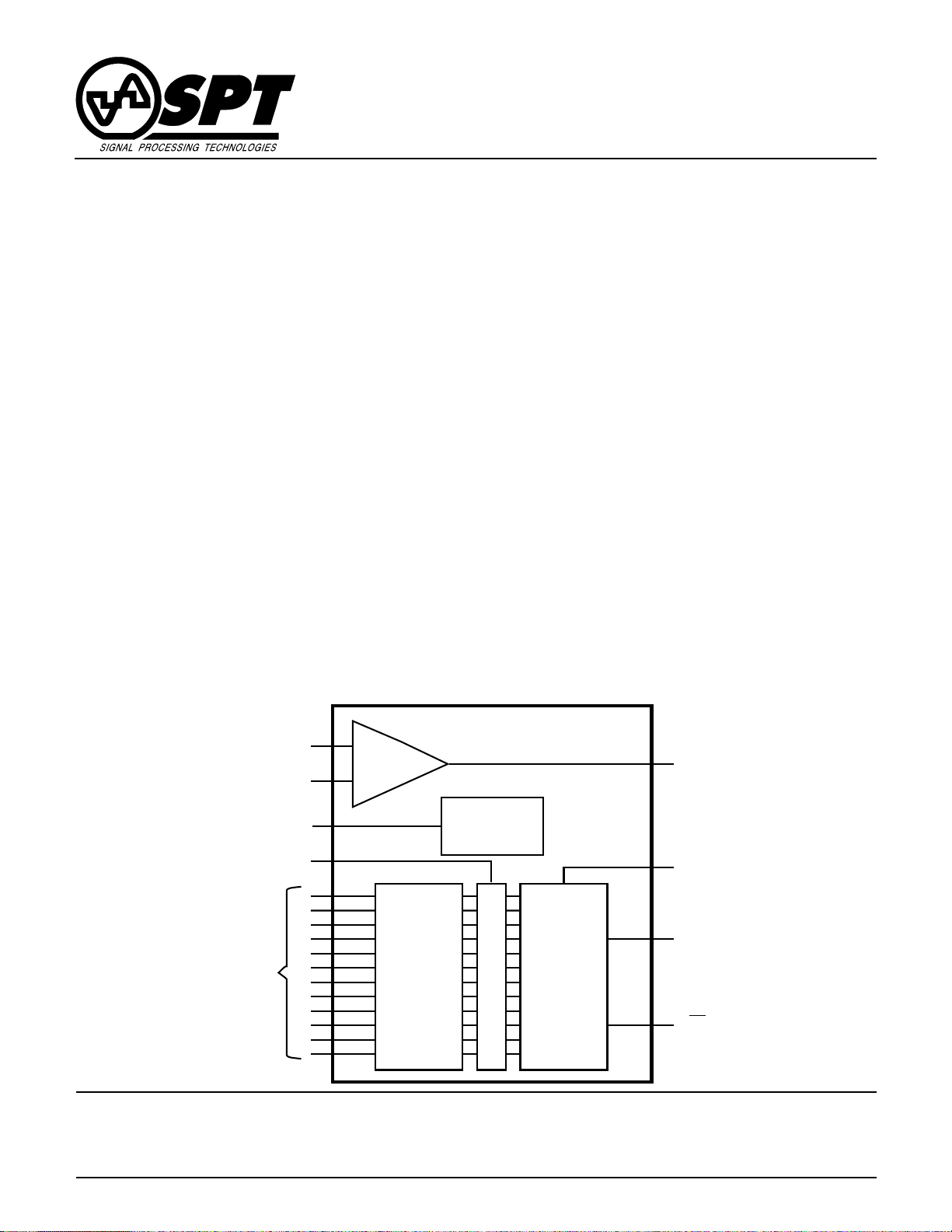
BLOCK DIAGRAM
R
Set
Control Amp In
Ref Out
Latch Enable
Digital
Inputs
D1
through
D12
+
Control
Amp
(MSB)
Decoders
and
Drivers
(LSB)
Internal
Voltage
Reference
Latches
Switch
Network
Control
Amp Out
Ref In
I
Out
I
Out
Signal Processing Technologies, Inc.
4755 Forge Road, Colorado Springs, Colorado 80907, USA
Phone: 719-528-2300 Fax: 719-528-2370 Web Site: http://www .spt.com e-mail: sales@spt.com

ABSOLUTE MAXIMUM RATINGS (Beyond which damage may occur)1 25 °C
Supply Voltages
Positive Supply Voltage (VCC)................................ +7 V
Negative Supply Voltage (VEE) .............................. –7 V
A/D Ground Voltage Differential ...........................0.5 V
Input Voltages
Digital Input Voltage
(D1–D12, Latch Enable)...............................0 V to V
Control Amp Input Voltage Range...............0 V to –4 V
Reference Input Voltage Range (V
) ........0 V to V
REF
Output Currents
Internal Reference Output Current.................... 500 µA
Control Amplifier Output Current.....................±2.5 mA
Temperature
Operating Temperature .......................... –40 to +85 °C
Junction Temperature ...................................... +150 °C
CC
Lead, Soldering (10 seconds) .........................+300 °C
Storage ................................................ –65 to +150 °C
EE
Note: 1. Operation at any Absolute Maximum Rating is not implied. See
Electrical Specifications for proper nominal applied conditions
in typical applications.
ELECTRICAL SPECIFICATIONS
TA = T
PARAMETERS CONDITIONS LEVEL MIN TYP MAX MIN TYP MAX UNITS
DC Performance
– T
MIN
, VCC = +5.0 V, V
MAX
= –5.2 V, R
EE
= 7.5 kΩ, Control Amp In = Ref Out, V
Set
= 0 V, unless otherwise specified.
OUT
TEST TEST SPT9713A SPT9713B
Resolution 12 12 Bits
Differential Linearity I ±0.5 ±0.75 ±1.0 ±1.25 LSB
Differential Linearity Max at Full Temp. VI ±1.5 ±2.0 LSB
Integral Linearity Best Fit I ±0.75 ±1.0 ±1.0 ±1.5 LSB
Integral Linearity Max at Full Temp. VI ±1.75 ±2.0 LSB
Output Capacitance +25 °C V 10 10 pF
Gain Error
1
+25 °C I 1.0 5.0 1.0 5.0 % FS
Full Temp. VI 8.0 8 . 0 % FS
Gain Error Tempco Full Temp. V 150 150 PPM/°C
Zero-Scale Offset Error +25 °C I 0.5 2.5 0.5 2.5 µA
Full Temp. VI 5.0 5 . 0 µA
Offset Drift Coefficient Full Temp. V 0.01 0.01 µA/°C
Output Compliance Voltage +25 °C IV –1.2 +2.0 –1.2 +2.0 V
Equivalent Output Resistance +25 °C IV 0.8 1.0 1.2 0.8 1.0 1.2 kΩ
Dynamic Performance
Conversion Rate +25 °C IV 100 10 0 MWPS
Settling Time t
ST
2
Output Propagation Delay t
Glitch Energy
4
Full Scale Output Current
D
5
+25 °C V 13 13 ns
3
+25 °C V 2 2 ns
+25 °C V 15 15 pV-s
+25 °C V 20.48 20.48 mA
Spurious-Free Dynamic Range6+25 °C
1.23 MHz; 10 MWPS 2 MHz Span V 70 70 dBc
5.055 MHz; 20 MWPS 2 MHz Span V 68 68 dBc
10.1 MHz; 50 MWPS 2 MHz Span V 68 68 dBc
16 MHz; 40 MWPS 10 MHz Span V 68 68 d Bc
Rise Time / Fall Time RL = 50 Ω V2 2ns
1
Gain is measured as a ratio of the full-scale current to I
2
Measured as voltage at mid-scale transition to ±0.024%; RL=50 Ω.
3
Measured from the rising edge of Latch Enable to where the output signal has left a 1 LSB error band.
4
Glitch is measured as the largest single transient.
5
Calculated using IFS = 128 x (Control Amp In / R
6
SFDR is defined as the difference in signal energy between the fundamental and worst case spurious frequencies in the output spectrum window ,
which is centered at the fundamental frequency and covers the indicated span.
Set
. The ratio is nominally 128.
Set
)
SPT9713
SPT
2 2/15/01

ELECTRICAL SPECIFICATIONS
TA = T
MIN
– T
MAX
, VCC = +5.0 V, V
= –5.2 V, R
EE
= 7.5 kΩ, Control Amp In = Ref Out, V
SET
= 0 V, unless otherwise specified.
OUT
TEST TEST SPT9713A SPT9713B
PARAMETERS CONDITIONS LEVEL MIN TYP MAX MIN TYP MAX UNITS
Power Supply Requirements
Positive Supply Voltage IV 4.75 5.0 +5.25 4.75 5.0 +5.25 V
Negative Supply Voltage IV –5.4 6 –5.2 –4.94 –5.46 –5.2 –4.94 V
Positive Supply Current (+5.0 V) +25 °C I 8 14 8 14 mA
Full Temp. VI 16 16 mA
Negative Supply Current (–5.2 V) +25 °C I 115 140 115 140 mA
Full Temp VI 148 148 mA
Nominal Power Dissipation V 640 640 m W
Power Supply Rejection Ratio ±5% of V
EE
and V
CC
I 30 100 30 100 µA/V
External Ref, +25 °C
Voltage Input and Control
Reference Input Impedance +25 °C V 3 3 kΩ
Ref. Multiplying Bandwidth +25 °C V 40 40 MHz
Internal Reference Voltage VI –1.15 –1.20 –1.25 –1.15 –1.20 –1.25 V
Internal Reference Voltage Drift Full V 50 50 ppm/°C
Amplifier Input Impedance +25 °C V 3 3 MΩ
Amplifier Input Bandwidth +25 °C V 1 1 MHz
Digital Inputs
Logic 1 Voltage Full Temp. VI 2.0 2.0 V
Logic 0 Voltage Full Temp. VI 0.8 0.8 V
Logic 1 Current Full Temp. VI 20 20 µA
Logic 0 Current Full Temp. VI 600 600 µA
Input Capacitance +25 °C V 3 3 pF
Input Setup Time – t
Input Setup Time – t
Input Hold Time – t
Input Hold Time – t
Latch Pulse Width – t
S
S
H
H
PWL, tPWH
+25 °C IV 3 2 3 2 ns
Full Temp. IV 3.5 3.5 ns
+25 °C IV 0.5 0 0.5 0 ns
Full Temp. IV 0.5 0.5 ns
+25 °C IV 5.0 4.0 5. 0 4.0 ns
TEST LEVEL CODES
All electrical characteristics are subject to the
following conditions:
All parameters having min/max specifications
are guaranteed. The Test Level column indicates the specific device testing actually performed during production and Quality Assurance inspection. Any blank section in the data
column indicates that the specification is not
tested at the specified condition.
LEVEL TEST PROCEDURE
I 100% production tested at the specified temperature.
II 100% production tested at TA = +25 °C, and sample tested at the
specified temperatures.
III QA sample tested only at the specified temperatures.
IV Parameter is guaranteed (but not tested) by design and characteri-
zation data.
V Parameter is a typical value for information pur poses only.
VI 100% production tested at TA = +25 °C. Parameter is guaranteed
over specified temperature range.
SPT
SPT9713
3 2/15/01
 Loading...