SPT SPT9689ACU, SPT9689AIC, SPT9689AIP, SPT9689BCU, SPT9689BIC Datasheet
...
FEATURES
SPT9689
DUAL ULTRAFAST VOLT AGE COMPARATOR
TECHNICAL DATA
FEBRUARY 20, 2001
APPLICATIONS
• 650 ps propagation delay
• 100 ps propagation delay variation
• 70 dB CMRR
• Low feedthrough and crosstalk
• Differential latch control
• ECL compatible
GENERAL DESCRIPTION
The SPT9689 is a
parator. The propagation delay variation is less than
100 ps from 5 to 50 mV input overdrive v oltage. The input
slew rate is 10 V/ns. The device utilizes a high precision
differential input stage with a common-mode range of
–2.5 V to +4.0 V.
Sub
nanosecond monolithic dual com-
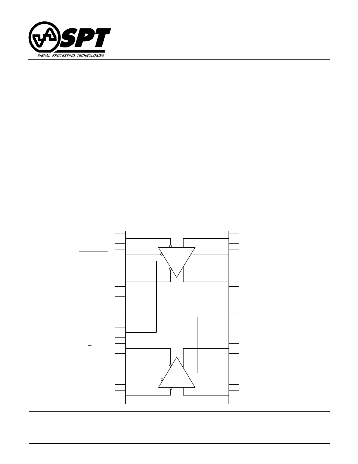
BLOCK DIAGRAM
INVERTING
INPUT
LATCH ENABLE
+
• Automated test equipment
• High-speed instrumentation
• Window comparators
• High-speed timing
• Line receivers
• High-speed triggers
• Threshold detection
• Peak detection
ECL-compatible complementary digital outputs are capable of driving 50 Ω terminated transmission lines and
providing 30 mA output drive. The SPT9689 is pin compatible with the SPT9687. It is a v ailable in 20-lead PLCC and
20-contact LCC packages over the industrial temperature
range. The SPT9689 is also available in die form.
NONINVERTING
INPUT
A
LATCH ENABLE
Q OUTPUT
V
V
GND
Q OUTPUT
LATCH ENABLE
INVERTING
INPUT
CC
EE
A
B
+
Q OUTPUT
GND
B
Q OUTPUT
LATCH ENABLE
NONINVERTING
INPUT
Signal Processing Technologies, Inc.
4755 Forge Road, Colorado Springs, Colorado 80907, USA
Phone: 719-528-2300 Fax: 719-528-2370 Web Site: http://www .spt.com e-mail: sales@spt.com

ABSOLUTE MAXIMUM RATINGS (Beyond which damage may occur)1 25 °C
Supply Voltages
Positive Supply Voltage (VCC to GND).... –0.5 to +6.0 V
Negative Supply Voltage (VEE to GND) ..–6.0 to +0.5 V
Ground V oltage Differential ....................–0.5 to +0.5 V
Input Voltages
Input Common Mode Voltage .................–4.0 to +5.0 V
Differential Input Voltage ........................ –3.0 to +3.0 V
Input Voltage, Latch Controls ....................V
to 0.5 V
EE
Output
Output Current ................................................... 30 mA
Temperature
Operating Temperature, ambient............ –40 to +85 °C
junction ..................... +150 °C
Lead Temperature, (soldering 60 seconds) ..... +300 °C
Storage Temperature............................ –65 to +150 °C
Note: 1. Operation at any Absolute Maximum Rating is not implied. See
Electrical Specifications for proper nominal applied conditions
in typical applications.
ELECTRICAL SPECIFICATIONS
T A = +25 °C, VCC = +5.0 V, VEE =–5.20 V , RL = 50 Ohm to –2 V, unless otherwise specified.
PARAMETERS CONDITIONS LEVEL MIN TYP MAX MIN TYP MAX UNITS
DC CHARACTERISTICS
Input Offset Voltage V
Input Offset Voltage V
Offset Voltage Tempco V 10 40 µV/°C
Input Bias Current I ±8 ±25 ±8 ±25 µA
Input Bias Current T
Input Offset Current I ±1.0 ±3.0 ±2.0 ±5.0 µA
Input Offset Current T
Positive Supply Current Dual I 18 30 18 35 mA
Negative Supply Current Dual I 40 55 40 60 mA
Positiv e Supply Voltage, V
Negative Supply Voltage, V
Input Common Mode Range V –2.5 +4.0 –2.5 +4.0 V
Latch Enable
Common Mode Range IV –2.0 0 –2.0 0 V
Open Loop Gain V 66 66 dB
Differential Input Resistance V 500 500 kΩ
Input Capacitance V 0.6 0.6 pF
Power Supply Sensitivity V 70 70 dB
Common Mode Rejection Ratio VCM=–2.5 to +4.0 V 70 70 dB
Power Dissipation Dual, Without Load I 350 425 350 4 75 mW
Power Dissipation Dual, With Load I 400 550 400 550 mW
Output High Level ECL 50 Ohms to –2 V I –1.00 –.81 –1.00 –.81 V
Output Low Level ECL 50 Ohms to –2 V I –1.95 –1.54 –1.95 –1.54 V
CC
TEST TEST SPT9689A SPT9689B
1
1
I –10 ±3.0 10 –25 ±12 25 mV
IV –15 ±4.5 15 –30 ±15 30 mV
IV ±12 ±38 ±12 ±38 µA
IV ±2.0 ±5.0 ±4.0 ±7.0 µA
IV 4.75 5.0 5.25 4.75 5.0 5.25 V
IV –4.95 –5.2 –5.45 –4.95 –5.2 –5.45 V
EE
=0, RS=0 Ohms
IN, CM
=0, RS=0 Ohms
IN, CM
T
MIN<TA<TMAX
MIN<TA<TMAX
MIN<TA<TMAX
AC CHARACTERISTICS
Propagation Delay 20 mV O.D. IV 650 850 750 950 ps
Latch Set-up Time V 150 300 150 300 ps
Latch to Output Delay 250 mV O.D. V 500 600 500 600 ps
Latch Pulse Width V 500 500 ps
Latch Hold Time V 0 0 ps
Rise Time 20% to 80% V 180 180 ps
Fall Time 20% to 80% V 80 80 ps
Slew Rate V 10 10 V/ns
Bandwidth –3 dB V 900 900 M Hz
1
RS = Source impedance
SPT9689
SPT
2 2/20/01

TEST LEVEL CODES
All electrical characteristics are subject to the
following conditions:
All parameters having min/max specifications
are guaranteed. The Test Level column indicates the specific device testing actually performed during production and Quality Assurance inspection. Any blank section in the data
column indicates that the specification is not
tested at the specified condition.
LEVEL TEST PROCEDURE
I 100% production tested at the specified temperature.
II 100% production tested at T
specified temperatures.
III QA sample tested only at the specified temperatures.
IV Parameter is guaranteed (but not tested) by design and characteri-
zation data.
V Parameter is a typical value for information purposes only.
VI 100% production tested at TA = +25 °C. Parameter is guaranteed
over specified temperature range.
= +25 °C, and sample tested at the
A
TIMING INFORMATION
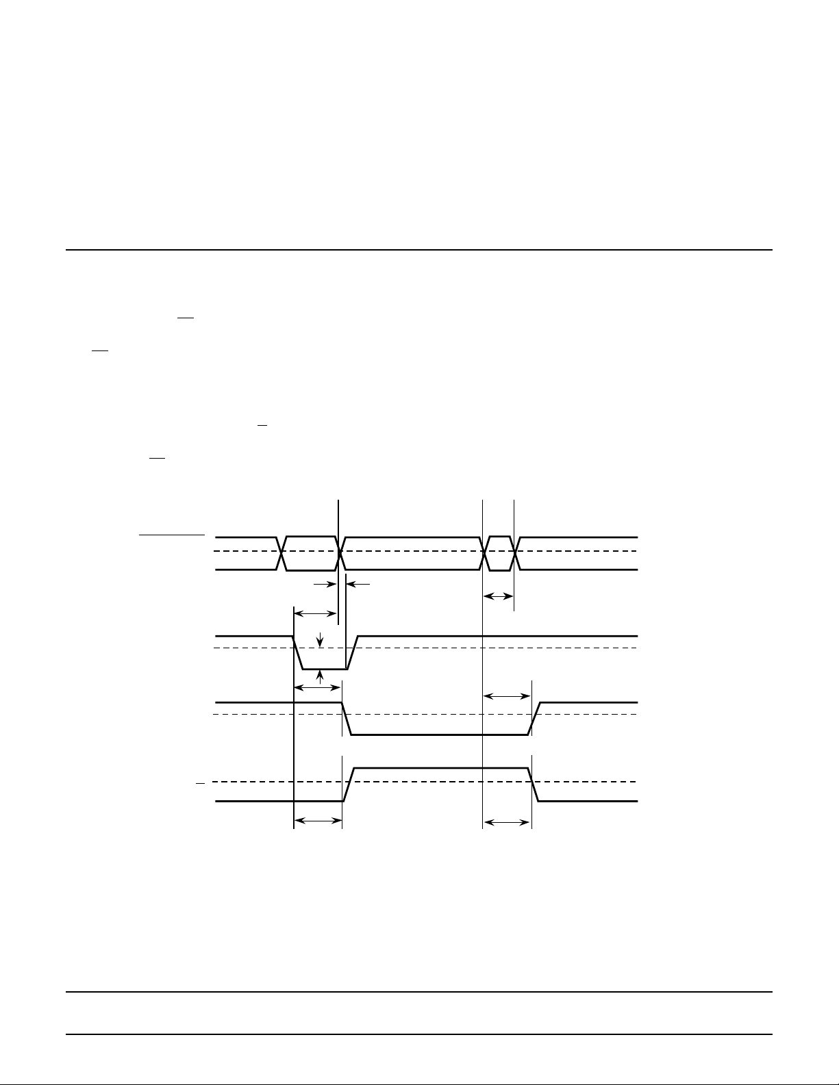
The timing diagram for the comparator is shown in figure
1. If LE is high and LE low in the SPT9689, the compar ator
tracks the input difference voltage. When LE is driven low
and LE high, the comparator outputs are latched into their
existing logic states.
The leading edge of the input signal (which consists of a
20 mV overdrive voltage) changes the comparator output
after a time of t
be maintained for a time tS (set-up time) before the LE falling edge and LE rising edge and held for time tH after the
Figure 1 – Timing Diagram
or t
pdL
Latch Enable
Latch Enable
Differential
Input Voltage
Output Q
(Q or Q). The input signal must
pdH
t
H
t
S
V
OD
t
pdL
falling edge for the compar ator to accept data. After tH, the
output ignores the input status until the latch is strobed
again. A minimum latch pulse width of tpL is needed for
strobe operation, and the output transitions occur after a
time of t
pLOH
or t
pLOL
.
The set-up and hold times are a measure of the time
required for an input signal to propagate through the first
stage of the comparator to reach the latching circuitry.
Input signals occurring before tS will be detected and held;
those occurring after tH will not be detected. Changes
between tS and tH may not be detected.
50%
t
pL
V
± V
REF
OS
t
pLOH
50%
SPT
Output Q
t
pdH
VIN+=100 mV (p-p), VOD=20 mV
3 2/20/01
t
pLOL
50%
SPT9689
 Loading...