

SPT SPT9405SCL Datasheet
SPT9405
SINGLE VIDEO DRIVER WITH LUMA OUTPUT
Signal Processing Technologies, Inc.
4755 Forge Road, Colorado Springs, Colorado 80907, USA
Phone: (719) 528-2300 FAX: (719) 528-2370
FEATURES
• Single Video Line Driver Chip
• Internal Clamp and Feedback Resistors
•RL=150 Ω (75 Ω Back-Terminated Cable)
• Power-Down Standby Mode
• Tiny 2.9 x 1.6 mm 6-Lead SOT23 Package
• Low Power Dissipation: 37.5 mW
•1 V
P-P
Input Range, 6 dB Voltage Gain
• Flat Response fIN = 100 kHz to 10 MHz (typical)
• Single +5 Volt Power Supply
APPLICATIONS
• Digital Video Disk
• Video Line Driver for Encoders
• Digital Video Tape Recorders
• Video Cassette Recorders
• PC Multimedia
• Consumer Video
GENERAL DESCRIPTION
The SPT9405 is a single video line driver chip that takes a
standard video signal as an analog input and provides a
buffered analog output for driving a 150 Ω load (75 Ω backterminated cable). The standard video input signal (1 V
P-P
) is
internally clamped and amplified 6 dB using internal circuitry
and feedback resistors to produce a 2 V
P-P
into an AC-
coupled 150 Ω load. The internal 1.5 kΩ resistor provides gain
compensation for low frequency signals. (See the typical
interface circuit diagram.)
The SPT9405 features a standby mode which draws only
120 µW of power. Nominal power dissipation (no input) is
typically 37.5 mW. It requires a single +5 V supply, operates
over the commercial temperature range (0 to +70 °C) and is
available in a tiny surface mount (2.9 x 1.6 mm) 6-lead SOT23 package.
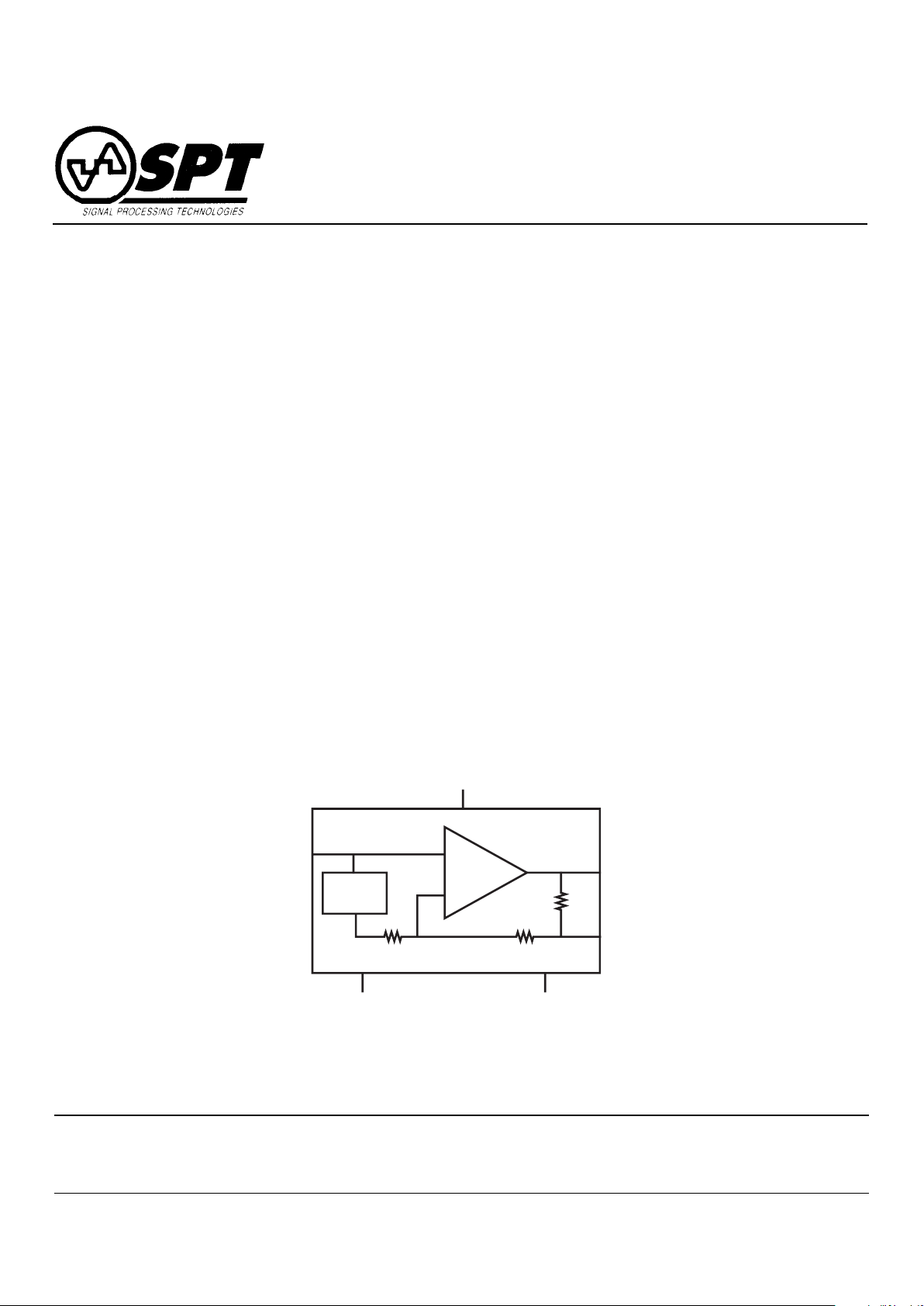
BLOCK DIAGRAM
Driver
Input
Output
V
CC
Standby GND
Clamp
1.25 V
5 kΩ 5 kΩ
1.5 kΩ
Output
FB

SPT
2 8/25/98
SPT9405
ELECTRICAL SPECIFICATIONS
TA = +25 °C, V
CC
= +5.0 V, VIN = 1.0 V
P-P
video signal, RL = 150 Ω, unless otherwise specified.
TEST TEST SPT9405
PARAMETERS CONDITIONS LEVEL MIN TYP MAX UNITS
Power Supply
Supply Current (I
CC
) No Input I 7.5 10 mA
V
CC
Voltage IV 4.5 5.0 5.5 V
Power Dissipation I 37.5 50 mW
Standby Current Pin 1 Grounded I 24.0 50 µA
Standby Power Dissipation Pin 1 Grounded I 120 250 µW
Digital Input
Digital Input (Low) Standby Pin 1 I 0.0 0.1 0.3 V
Digital Input (High) Standby Pin 1 I 1.8 2.0 V
CC
V
Bias Voltage
Clamp Voltage Pin 4 I 1.05 1.25 1.45 V
Dynamic Performance
Voltage Gain fIN = 1 MHz I 5.4 5.9 6.4 dB
Differential Gain Ramp Input 3.58 MHz I -3.0 -0.6 +3.0 %
Differential Phase Ramp Input 3.58 MHz I -3.0 -0.2 +3.0 Degrees
Frequency Response fIN = 1 to 5 MHz V -0.5 dB
ABSOLUTE MAXIMUM RATINGS (Beyond which damage may occur)
(1)
25 °C
Supply Voltages
VCC.......................................................................+6.0 V
Maximum Power Dissipation
P
D
....................................................................................
150 mW
Thermal Impedance (TA=+25 °C and above)
Θ
CA
............................................................................
1.2 mW/°C
Temperature
Operating Temperature ................................. 0 to +70 °C
Storage Temperature................................-55 to +150 °C
Note: 1. Operation at any Absolute Maximum Rating is not implied. See Electrical Specifications for proper nominal
applied conditions in typical applications.
TEST PROCEDURE
100% production tested at the specified temperature.
100% production tested at TA = +25 °C, and sample tested
at the specified temperatures.
QA sample tested only at the specified temperatures.
Parameter is guaranteed (but not tested) by design and
characterization data.
Parameter is a typical value for information purposes only.
100% production tested at T
A
= +25 °C. Parameter is
guaranteed over specified temperature range.
TEST LEVEL
I
II
III
IV
V
VI
TEST LEVEL CODES
All electrical characteristics are subject to the following
conditions:
All parameters having min/max specifications are guaranteed. The Test Level column indicates the specific
device testing actually performed during production and
Quality Assurance inspection. Any blank section in the
data column indicates that the specification is not tested
at the specified condition.
 Loading...