

SPT SPT7910SCJ, SPT7910SCU Datasheet
SPT7910
12-BIT, 10 MSPS, ECL, A/D CONVERTER
FEATURES
• Monolithic
• 12-Bit 10 MSPS Converter
• 67 dB SNR @ 500 kHz Input
• On-Chip Track/Hold
• Bipolar ±2.0 V Analog Input
• Low Power (1.4 W Typical)
• 5 pF Input Capacitance
• ECL Outputs
GENERAL DESCRIPTION
The SPT7910 analog-to-digital converter is industry's first
12-bit monolithic analog-to-digital converter capable of sample
rates greater than 10 MSPS. On board input buffer and track/
hold function assures excellent dynamic performance without the need for external components. Drive requirement
problems are minimized with an input capacitance of only
5 pF.
Inputs and outputs are ECL to provide a higher level of noise
immunity in high speed system applications. An overrange
APPLICATIONS
• Radar Receivers
• Professional Video
• Instrumentation
• Medical Imaging
• Electronic Warfare
• Digital Communications
• Digital Spectrum Analyzers
• Electro-Optics
output signal is provided to indicate overflow conditions.
Output data format is straight binary. Power dissipation is
very low at only 1.4 watts with power supply voltages of +5.0
and -5.2 volts. The SPT7910 also provides a wide input
voltage range of ±2.0 volts.
The SPT7910 is available in a 32-lead ceramic sidebrazed
DIP package and in die form. A commercial temperature
range of 0 to +70 °C is currently offered.
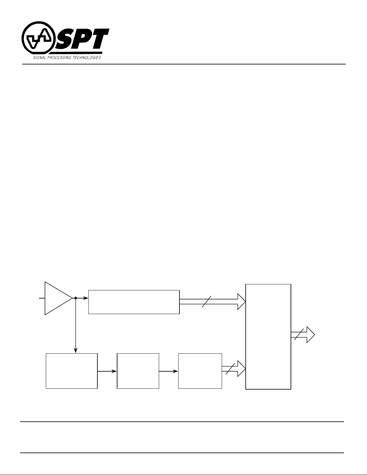
BLOCK DIAGRAM
V
IN
INPUT
BUFFER
ANALOG GAIN
COMPRESSION
PROCESSOR
Signal Processing Technologies, Inc.
4-BIT FLASH
CONVERTER
TRACK AND HOLD
AMPLIFIERS
ASYNCHRONOUS
SAR
4
CORRECTION,
OUTPUT ECL
8
4755 Forge Road, Colorado Springs, Colorado 80907, USA
Phone: (719) 528-2300 FAX: (719) 528-2370
ERROR
DECODING
AND
DRIVERS
DIGITAL
OUTPUT
12

ABSOLUTE MAXIMUM RATINGS (Beyond which damage may occur)1 25 °C
Supply Voltages
VCC............................................................... -0.3 to +6 V
Output
Digital Outputs .............................................. 0 to -30 mA
VEE............................................................... +0.3 to -6 V
Temperature
Input Voltages
Analog Input............................................... VFB≤VIN≤V
VFT, VFB. ................................................... +3.0 V, -3.0 V
Reference Ladder Current .....................................12 mA
FT
Operating Temperature ................................... 0 to 70 °C
Junction Temperature ........................................... 175 °C
Lead Temperature, (soldering 10 seconds).......... 300 °C
Storage Temperature................................-65 to +150 °C
Note: 1. Operation at any Absolute Maximum Rating is not implied. See Electrical Specifications for proper nominal
applied conditions in typical applications.
ELECTRICAL SPECIFICATIONS
TA=T
unless otherwise specified.
PARAMETERS CONDITIONS LEVEL MIN TYP MAX UNITS
Resolution 12 Bits
DC Accuracy (+25 °C)
Analog Input
Reference Input
Timing Characteristics
Dynamic Performance
to T
MIN
Integral Nonlinearity ± Full Scale V ±2.0 LSB
Differential Nonlinearity 250 kHz Sample Rate V ±0.8 LSB
No Missing Codes VI Guaranteed
Input Voltage Range VI ±2.0 V
Input Bias Current VI 30 60 µA
Input Resistance VIN=0 V VI 100 300 kΩ
Input Capacitance V 5 pF
Input Bandwidth 3 dB Small Signal V 120 MHz
+FS Error V ±5.0 LSB
-FS Error V ±5.0 LSB
Reference Ladder Resistance VI 500 800 Ω
Reference Ladder Tempco V 0.8 Ω/°C
Maximum Conversion Rate VI 10 MHz
Overvoltage Recovery Time V 20 ns
Pipeline Delay (Latency) IV 1 Clock Cycle
Output Delay V 5 ns
Aperture Delay Time V 1 ns
Aperture Jitter Time V 5 ps-RMS
Effective Number of Bits
fIN=500 kHz 10.2 Bits
fIN=1.0 MHz 10.0 Bits
fIN=3.58 MHz 9.5 Bits
, VCC=+5.0 V, VEE=-5.2 V, DVCC=+5.0 V, VIN=±2.0 V, VSB=-2.0 V, VST=+2.0 V, f
MAX
TEST TEST SPT7910
10 MHz, 50% clock duty cycle,
CLK=
SPT
SPT7910
2 3/11/97

ELECTRICAL SPECIFICATIONS
TA=T
MIN
to T
, VCC=+5.0 V, VEE=-5.2 V, DVCC=+5.0 V, VIN=±2.0 V, VSB=-2.0 V, VST=+2.0 V, f
MAX
10 MHz, 50% clock duty cycle,
CLK=
unless otherwise specified.
TEST TEST SPT7910
PARAMETERS CONDITIONS LEVEL MIN TYP MAX UNITS
Dynamic Performance
Signal-To-Noise Ratio
(without Harmonics)
f
=500 kHz +25 °C I 64 67 dB
IN
to T
T
MIN
=1 MHz +25 °C I 64 66 dB
f
IN
T
MIN
=3.58 MHz +25 °C I 62 64 dB
f
IN
T
MIN
Harmonic Distortion
1
to T
to T
MAX
MAX
MAX
IV 58 61 dB
IV 58 60 dB
IV 58 60 dB
fIN=500 kHz +25 °C I 63 66 dB
to T
T
MIN
=1.0 MHz +25 °C I 63 65 dB
f
IN
T
MIN
=3.58 MHz +25 °C I 59 61 dB
f
IN
T
MIN
to T
to T
MAX
MAX
MAX
IV 59 62 dB
IV 59 61 dB
IV 57 59 dB
Signal-to-Noise and Distortion
=500 kHz +25 °C I 60 63 dB
f
IN
T
to T
MIN
=1.0 MHz +25 °C I 60 62 dB
f
IN
T
MIN
=3.58 MHz +25 °C I 57 59 dB
f
IN
T
MIN
Spurious Free Dynamic Range
Differential Phase
Differential Gain
3
3
2
+25 °C V 74 dB
+25 °C V 0.2 Degree
+25 °C V 0.7 %
to T
to T
MAX
MAX
MAX
IV 55 58 dB
IV 55 57 dB
IV 54 56 dB
Digital Inputs
Logic 1 Voltage VI -1.1 V
Logic 0 Voltage VI -1.5 V
Maximum Input Current Low VI -500 ±200 +750 µA
Maximum Input Current High VI -500 ±300 +750 µA
Pulse Width Low (CLK) IV 30 ns
Pulse Width High (CLK) IV 30 300 ns
Digital Outputs
Logic 1 Voltage 50 Ω to -2 V VI -1.1 -0.8 V
Logic 0 Voltage 50 Ω to -2 V VI -1.8 -1.5 V
Power Supply Requirements
Voltages V
Currents I
-V
-I
CC
EE
CC
EE
IV +4.75 +5.25 V
IV -4.95 -5.45 V
VI 150 190 mA
VI 125 160 mA
Power Dissipation Outputs Open VI 1.4 1.8 W
Power Supply Rejection Ratio (5 V±0.25 V, -5.2 V ±0.25 V) V 1.0 LSB
Typical thermal impedances (unsoldered, in free air): 32L sidebrazed DIP. θja = 50 °C/W.
1
64 distortion BINS from 4096 pt FFT.
2
fIN = 1 MHz.
3
fIN = 3.58 and 4.35 MHz.
SPT
3 3/11/97
SPT7910
A
A
A
A
TEST LEVEL CODES
TEST LEVEL
TEST PROCEDURE
All electrical characteristics are subject to the
following conditions:
All parameters having min/max specifications
are guaranteed. The Test Level column indicates the specific device testing actually performed during production and Quality Assurance inspection. Any blank section in the data
column indicates that the specification is not
tested at the specified condition.
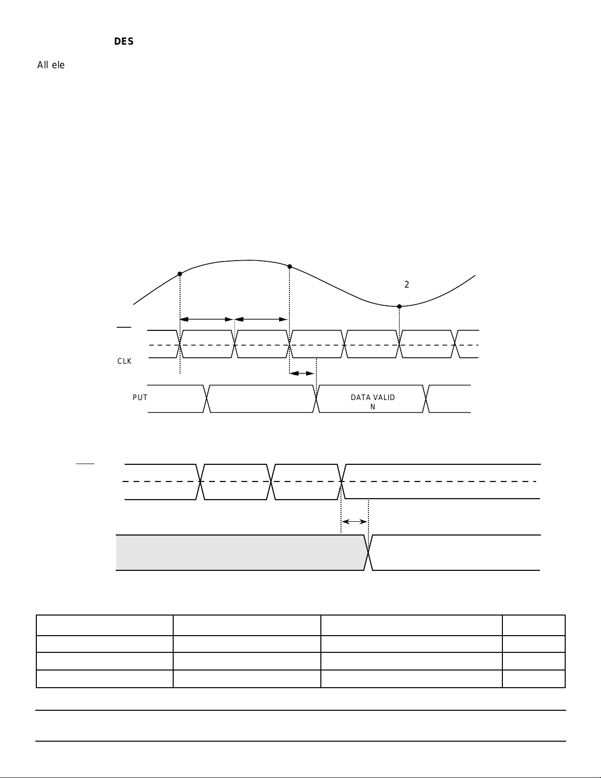
Figure 1A: Timing Diagram
N
tt
pwH pwL
CLK
III
IV
VI
I
II
V
N+1
100% production tested at the specified temperature.
100% production tested at TA=25 °C, and sample
tested at the specified temperatures.
QA sample tested only at the specified temperatures.
Parameter is guaranteed (but not tested) by design
and characterization data.
Parameter is a typical value for information purposes
only.
100% production tested at TA = 25 °C. Parameter is
guaranteed over specified temperature range.
N+2
CLK
OUTPUT
DATA
Figure 1B: Single Event Clock
CLK
CLK
OUTPUT
DATA
Table I - Timing Parameters
PARAMETERS DESCRIPTION MIN TYP MAX UNITS
t
d
t
pwH
t
pwL
t
d
N-2 N-1
CLK to Data Valid Prop Delay - 5 ns
CLK High Pulse Width 30 - 300 ns
CLK Low Pulse Width 30 - - ns
DATA VALID
N
t
d
DATA VALID
N+1
DATA VALID
SPT
SPT7910
4 3/11/97
 Loading...