SPT SPT7870SCU, SPT7870SIQ Datasheet

SPT7870
A
A
A
A
A
A
A
A
A
A
A
A
A
A
A
A
A
A
A
A
A
A
A
A
A
A
A
A
A
A
10-BIT, 100 MSPS ECL A/D CONVERTER
FEATURES
• 10-Bit, 100 MSPS Analog-to-Digital Converter
• Monolithic Bipolar
• Single-Ended Bipolar Analog Input
• -1.0 V to +1.0 V Analog Input Range
• Internal Sample-and-Hold
• Internal Voltage Reference
• Programmable Data Output Formats
• Single Ended ECL/PECL Outputs
• TTL Version Available as the SPT7871
GENERAL DESCRIPTION
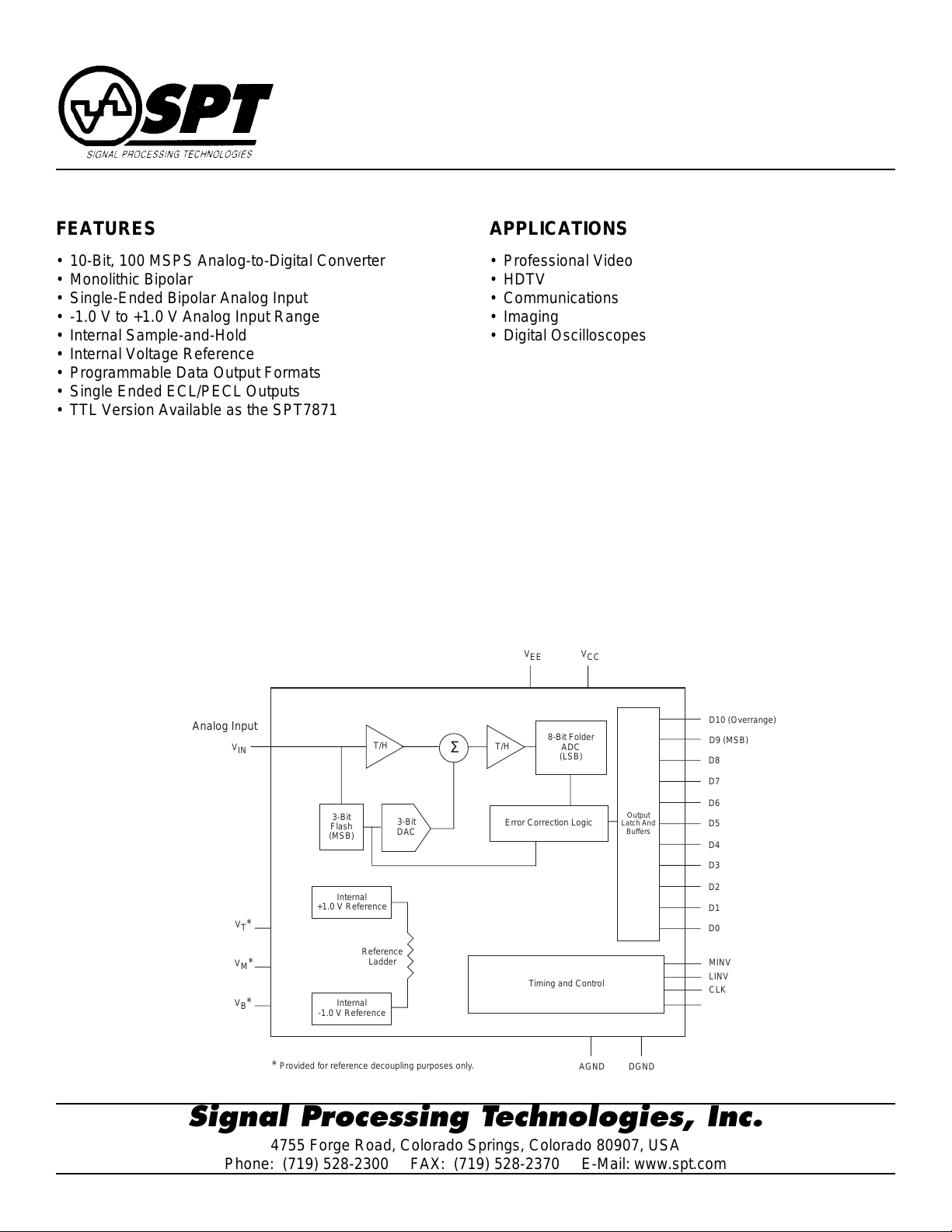
The SPT7870 is a 10-bit, 100 MSPS analog-to-digital converter, with a two stage sub-ranging flash/folder architecture.
The bipolar, single-ended analog input provides an easy
interface for most applications. Programmable data output
formats provide additional ease of implementation and flexibility. The device supports high-speed ECL- and PECL-level
outputs.
BLOCK DIAGRAM
AAAAAAAAAAAAAAAAAAAAAAAAAAAAAA
AAAAAAAAAAAAAAAAAAAAAAAAAAAAAA
AAAAAAAAAAAAAAAAAAAAAAAAAAAAAA
AAAAAAAAAAAAAAAAAAAAAAAAAAAAAA
IN
AAAAAAAAAAAAAAAAAAAAAAAAAAAAAA
T/H
AAAAAAAAAAAAAAAAAAAAAAAAAAAAAA
AAAAAAAAAAAAAAAAAAAAAAAAAAAAAA
AAAAAAAAAAAAAAAAAAAAAAAAAAAAAA
AAAAAAAAAAAAAAAAAAAAAAAAAAAAAA
AAAAAAAAAAAAAAAAAAAAAAAAAAAAAA
AAAAAAAAAAAAAAAAAAAAAAAAAAAAAA
3-Bit
Flash
(MSB)
3-Bit
DAC
AAAAAAAAAAAAAAAAAAAAAAAAAAAAAA
AAAAAAAAAAAAAAAAAAAAAAAAAAAAAA
AAAAAAAAAAAAAAAAAAAAAAAAAAAAAA
AAAAAAAAAAAAAAAAAAAAAAAAAAAAAA
AAAAAAAAAAAAAAAAAAAAAAAAAAAAAA
AAAAAAAAAAAAAAAAAAAAAAAAAAAAAA
V
*
T
AAAAAAAAAAAAAAAAAAAAAAAAAAAAAA
AAAAAAAAAAAAAAAAAAAAAAAAAAAAAA
AAAAAAAAAAAAAAAAAAAAAAAAAAAAAA
V
*
M
AAAAAAAAAAAAAAAAAAAAAAAAAAAAAA
Internal
AAAAA
+1.0 V Reference
Reference
AAAAAAAAAAAAAAAAAAAAAAAAAAAAAA
AAAAAAAAAAAAAAAAAAAAAAAAAAAAAA
V
*
B
AAAAAAAAAAAAAAAAAAAAAAAAAAAAAA
AAAAAAAAAAAAAAAAAAAAAAAAAAAAAA
Internal
AAAAA
-1.0 V Reference
Ladder
*
Provided for reference decoupling purposes only.
4755 Forge Road, Colorado Springs, Colorado 80907, USA
Analog Input
V
Signal Processing Technologies, Inc.
Phone: (719) 528-2300 FAX: (719) 528-2370 E-Mail: www.spt.com
APPLICATIONS
• Professional Video
• HDTV
• Communications
• Imaging
• Digital Oscilloscopes
The resolution and performance of this device makes it well
suited for professional video and HDTV applications. The onchip track-and-hold provides for excellent AC performance
enabling this device to be a converter of choice for RF
communications and digital sampling oscilloscopes. The
SPT7870 is available in a 44L cerquad package in the
industrial temperature range and in die form.
V
EE
T/H
Σ
Error Correction Logic
AAAAAAAAAAAAA
AAAAAAAAAAAAA
Timing and Control
AAAAAAAAAAAAA
V
8-Bit Folder
ADC
(LSB)
AGND DGND
CC
Output
Latch And
Buffers
D10 (Overrange)
D9 (MSB)
D8
D7
D6
D5
D4
D3
D2
D1
D0
MINV
LINV
CLK
NCLK

ABSOLUTE MAXIMUM RATING (Beyond which damage may occur)
1
Supply Voltages
V
...........................................................................
CC
V
.............................................................................
EE
0 to +6.5 V
0 to -6.5 V
Output
Digital Outputs ......................................... +30 to -30 mA
Temperature
Input Voltages
Analog Input............................................. VEE≤VIN≤V
LINV/MINV Inputs ......................... -0.5 V to VCC + 0.5 V
CLK/NCLK Inputs........................................... VEE to 0 V
CC
Operating Temperature .............................-40 to + 85 °C
Junction Temperature ........................................ + 175 °C
Lead, Soldering (10 seconds)............................ + 300 °C
Storage ....................................................-60 to + 150 °C
Note: 1. Operation at any Absolute Maximum Ratings is not implied. See Electrical Specifications for proper nominal applied
conditions in typical applications.
ELECTRICAL SPECIFICATIONS
TA=+25 °C, VCC=+5.0 V, VEE=-5.2 V, VIN=±1.0 V, f
TEST TEST
PARAMETERS CONDITIONS LEVEL MIN TYP MAX UNITS
DC Performance
Resolution 10 Bits
Differential Linearity f
Integral Linearity, Best Fit f
No Missing Codes f
Analog Input
Input Voltage Range V ±1.0 V
Input Bias Current I -100 25 100 µA
Input Resistance I 50 150 kΩ
Input Capacitance V 5 pF
Input Bandwidth Full Power IV 150 180 MHz
±FS Offset Error I ±20 ±100 mV
Timing Characteristics
Maximum Conversion Rate IV 100 MSPS
Minimum Conversion Rate V 2 MSPS
Pipeline Delay (Latency) IV 2 Clock
Transient Response V 10 ns
Overvoltage Recovery Time V 10 ns
Output Delay (t
Aperture Delay Time V 1 ns
Aperture Jitter Time V 5 ps (rms)
Dynamic Performance
Effective Number of Bits
=10 MHz I 8.1 8.5 Bits
f
IN
= 25 MHz I 8.1 8.5 Bits
f
IN
fIN = 25 MHz f
= 50 MHz I 7.4 7.8 Bits
f
IN
fIN = 50 MHz f
Signal-To-Noise Ratio
=10 MHz I 52 55 dB
f
IN
= 25 MHz I 52 54 dB
f
IN
fIN = 25 MHz f
= 50 MHz I 52 54 dB
f
IN
fIN = 50 MHz f
Total Harmonic Distortion
fIN = 10 MHz I -56 -63 dBc
= 25 MHz I -55 -60 dBc
f
IN
fIN = 25 MHz f
= 50 MHz I -47 -51 dBc
f
IN
fIN = 50 MHz f
)V3ns
d
1
Clock
Clock
Full Temperature V ±2.5 LSB
Clock
Full Temperature V 100 kΩ
Clock
Clock
Clock
Clock
Clock
Clock
=80 MHz, 50% clock duty cycle, unless otherwise specified.
Clock
= 6.4 MHz I -1.0 ±0.5 +1.25 LSB
= 6.4 MHz I ±1.0 ±2.0 LSB
= 6.4 MHz I Guaranteed
= 100 MHz V 8.0 Bits
= 100 MHz V 7.5 Bits
= 100 MHz V 51 dB
= 100 MHz V 50 dB
= 100 MHz V -56 dBc
= 100 MHz V -50 dBc
SPT
SPT7870
2 9/8/98

ELECTRICAL SPECIFICATIONS
TA=+25 °C, VCC=+5.0 V, VEE=-5.2 V, VIN=±1.0 V, f
TEST TEST
PARAMETERS CONDITIONS LEVEL MIN TYP MAX UNITS
Dynamic Performance
Signal-to-Noise & Distortion (SINAD)
fIN = 10 MHz I 51 54 dB
fIN = 25 MHz I 51 53 dB
fIN = 25 MHz f
fIN = 50 MHz I 46.5 48 dB
fIN = 50 MHz f
Spurious Free Dynamic Range
fIN = 10 MHz V 65 dB FS
fIN = 25 MHz V 62 dB FS
fIN = 50 MHz V 52 dB FS
Two-Tone Intermodulation
Dist. Rejection
Differential Phase V 0.5 Degree
Differential Gain V 1 %
Power Supply Requirements
+VCC Supply Voltage IV 4.75 5.0 5.25 V
- VEE Supply Voltage IV -4.95 -5.2 -5.45 V
+VCC Supply Current VI 127 151 mA
- VEE Supply Current VI 202 240 mA
Power Dissipation VI 1.7 2.0 W
Power Supply Rejection Ratio IV 30 dB
Digital Inputs
LINV, MINV V CMOS/TTL Logic
Clock Inputs
Logic 1 Voltage VI -1.1 V
Logic 0 Voltage VI -1.5 V
Maximum Input Current Low VI -100 +100 µA
Maximum Input Current HIgh VI -100 +100 µA
Pulse Width Low (t
Pulse Width High (t
Rise/Fall Time 20% to 80% IV 1.5 ns
Digital Outputs
Logic 1 Voltage (ECL) 50 Ω to -2 V, DGND=0.0 V VI -1.1 -0.9 V
Logic 0 Voltage (ECL) 50 Ω to -2 V, DGND=0.0 V VI -1.7 -1.5 V
Logic 1 Voltage (PECL) 50 Ω to +3 V, DGND=+5.0 V IV 3.9 4.1 V
Logic 0 Voltage (PECL) 50 Ω to +3 V, DGND=+5.0 V IV 3.3 3.5 V
t
rise
t
fall
1
2048 pt FFT using distortion harmonics 2 through 10.
2
Measured as a second order (f1-f2) intermodulation product from a two-tone test, with each input tone at 0 dBm.
2
) IV 4.0 250 ns
pwl
) IV 4.0 250 ns
pwh
Clock
Clock
10% to 90% V 2.0 ns
10% to 90% V 2.0 ns
=80 MHz, 50% clock duty cycle, unless otherwise specified.
Clock
= 100 MHz V 50 dB
= 100 MHz V 47 dB
V -65 dBc
TEST LEVEL CODES
All electrical characteristics are subject to the
following conditions:
All parameters having min/max specifications
are guaranteed. The Test Level column indicates the specific device testing actually performed during production and Quality Assurance inspection. Any blank section in the data
column indicates that the specification is not
tested at the specified condition.
SPT
TEST LEVEL
I
II
III
IV
V
VI
3 9/8/98
TEST PROCEDURE
100% production tested at the specified temperature.
100% production tested at TA=25 °C, and sample
tested at the specified temperatures.
QA sample tested only at the specified temperatures.
Parameter is guaranteed (but not tested) by design
and characterization data.
Parameter is a typical value for information purposes
only.
100% production tested at TA = 25 °C. Parameter is
guaranteed over specified temperature range.
SPT7870
 Loading...