SPT SPT7864SIR Datasheet

Signal Processing Technologies, Inc.
4755 Forge Road, Colorado Springs, Colorado 80907, USA
Phone: 719-528-2300 Fax: 719-528-2370 Web Site: http://www .spt.com e-mail: sales@spt.com
SPT7864
10-BIT, 40 MSPS A/D CONVERTER
PRELIMINARY INFORMATION
APPLICATIONS
• High-speed applications where low power dissipation is
required
• Video imaging
• Medical imaging
• Radar receivers
• IR imaging
• Digital communications
FEATURES
• 40 MSPS maximum sample r ate
• 9.5 eff ectiv e n umber of bits at ƒIN = 10 MHz and
ƒS = 40 MSPS
•2 V
P-P
full-scale input range
• Diff erential input 2.5 V common mode
• Internal or external voltage ref erence
• Common-mode v oltage reference output
• +3.3 V / +5 V digital output logic compatibility
• +5 V analog power supply
GENERAL DESCRIPTION
The SPT7864 is a 10-bit, 40 MSPS analog-to-digital converter with low power dissipation at only 395 mW typical at
40 MSPS with a power supply of +5.0 V. The digital outputs
are +3 V or +5 V, and are user selectable. The SPT7864
has incorporated proprietary circuit design and CMOS
processing technologies to achieve its advanced performance. Inputs and outputs are TTL/CMOS compatible to
interface with TTL/CMOS logic systems. Output data format is straight binary.
The SPT7864 is available in a 28-lead SSOP package
over the industrial temperature range.
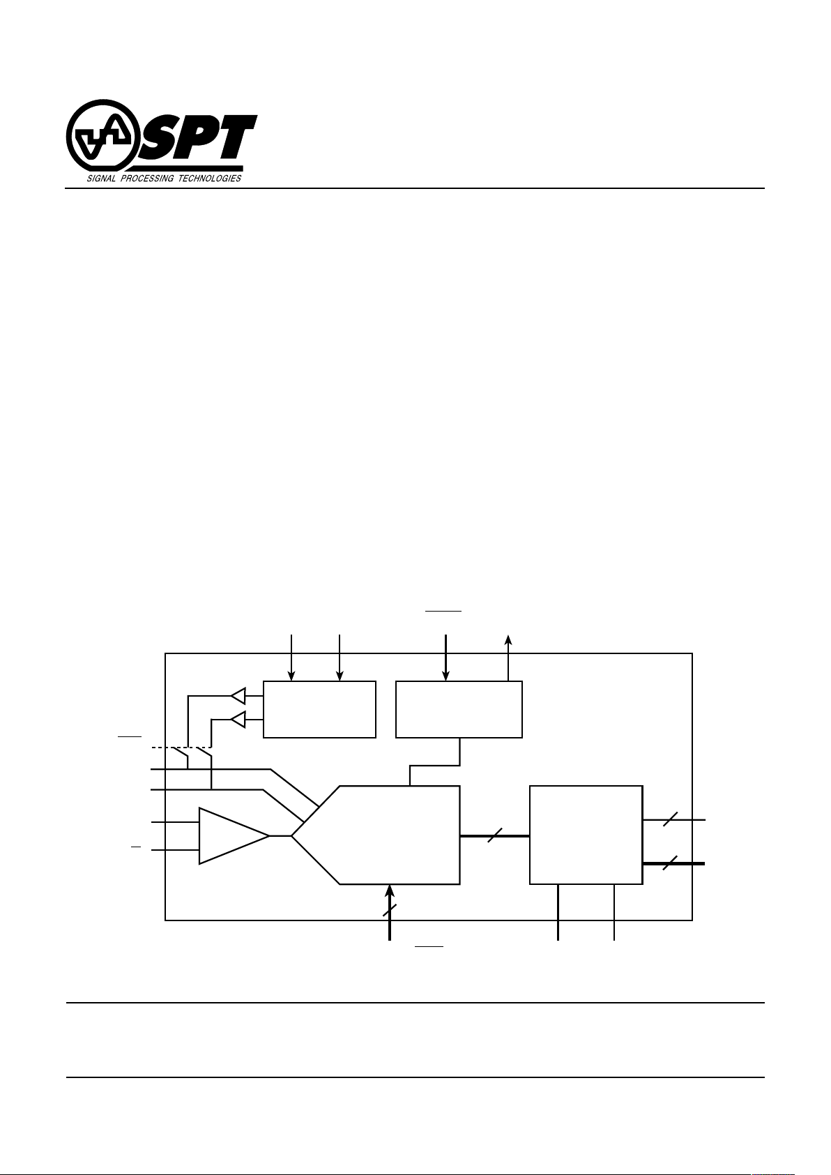
BLOCK DIAGRAM
Bias
Cell
V
CM
V
DD
GND
10-BIT
40 MSPS
ADC
THA
V
IN
Data
Output
Latches
& Buffers
10
10
GND OV
DD
Bandgap
Reference
2
CLK, CLK
V
IN
REF
H
REF
L
Sleep
1
OR
EXT/INT
D0D9

SPT
2 8/15/00
SPT7864
ABSOLUTE MAXIMUM RATINGS (Beyond which damage may occur)1 25 °C
Supply V oltages
VDD....................................................................... TBD
OVDD..................................................................... TBD
Input V oltages
Analog Input .......................................................... TBD
CLK Input .............................................................. TBD
Note: 1. Operation at any Absolute Maximum Rating is not implied. See Electrical Specifications for proper nominal applied conditions in typical
applications.
Output
Digital Outputs....................................................... TBD
T emperature
Operating Temperature ........................... –40 to +85 °C
Storage Temperature ............................ –65 to +150 °C
ELECTRICAL SPECIFICATIONS
TA=T
MIN
to T
MAX
, VDD=+5.0 V , ƒS=40 MSPS, V
RHS
=3.0 V, V
RLS
=2.0 V, unless otherwise specified.
TEST TEST SPT7864
PARAMETERS CONDITIONS LEVEL MIN TYP MAX UNITS
Resolution 10 Bits
DC Accuracy
Differential Linearity Error (DLE) @ +25 °C V ±0.4 LSB
full temperature ±0.75 LSB
Integral Linearity Error (ILE) @ +25 °C V ±0.5 LSB
full temperature ±1.0 LSB
No Missing Codes VI Guaranteed
Analog Input
Input Voltage Range (Differential) V ±1 V
Input Common Mode V 2.5 V
Input Capacitance V 2 pF
Common Mode Rejection Ratio (CMRR) TBD
Timing Characteristics
Conversion Rate VI 40 MSPS
Pipeline Delay (Latency) IV 7 clocks
Output Delay (t
D
) IV TBD TBD TBD ns
Aperture Delay Time V TBD ns
Aperture Jitter Time V TBD ps (rms)
Dynamic Performance
Effective Number of Bits (ENOB)
ƒ
IN
= 10 MHz, ƒ
CLK
= 40 MSPS 25 °C I 9.3 9.5 Bits
–40 °C to +85 °C IV 9.0 9.2 Bits
Signal-to-Noise Ratio (SNR)
ƒ
IN
= 10 MHz, ƒ
CLK
= 40 MSPS 25 °C I 58 59 d B
–40 °C to +85 °C IV 57 5 8 dB
Total Harmonic Distortion (THD)
ƒ
IN
= 10 MHz, ƒ
CLK
= 40 MSPS 25 °C I –71 –68 dB
–40 °C to +85 °C IV –70 –67 dB
Signal-to-Noise and Distortion (SINAD)
ƒ
IN
= 10 MHz, ƒ
CLK
= 40 MSPS 25 °C I 58 59 d B
–40 °C to +85 °C IV 56 5 7 dB
Spurious Free Dynamic Range (SFDR)
ƒ
IN
= 10 MHz, ƒ
CLK
= 40 MSPS 25 °C I 70 73 d B
–40 °C to +85 °C IV 68 7 1 dB
 Loading...