

SPT SPT7851SIT Datasheet
SPT7851
10-BIT, 20 MSPS, 79 mW A/D CONVERTER
FEATURES
• 10-Bit, 20 MSPS Analog-to-Digital Converter
• Monolithic CMOS
• Internal Track-and-Hold
• Low Input Capacitance: 1.4 pF
• Low Power Dissipation: 79 mW
• 2.8 – 3.6 V Power Supply Range
• TTL-Compatible Outputs
• –40 °C to +85 °C Operation
GENERAL DESCRIPTION
The SPT7851 10-bit, 20 MSPS analog-to-digital converter
has a pipelined converter architecture built in a CMOS process. It delivers high performance with a typical power dissipation of only 79 mW. With low distortion and high dynamic
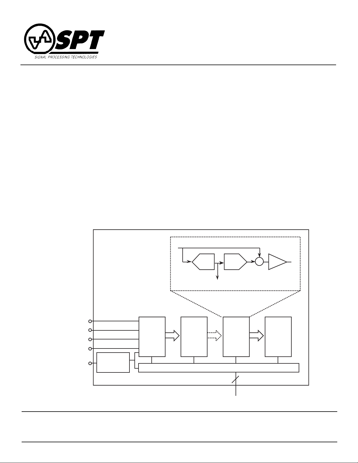
BLOCK DIAGRAM
APPLICATIONS
• CCD Imaging Cameras and Sensors
• Medical Imaging
• RF Communications
• Document and Film Scanners
• Electro-Optics
• Transient Signal Analysis
• Handheld Equipment
range, this device offers the performance needed for imaging, multimedia, telecommunications and instrumentation
applications.
The SPT7851 is available in a 44-lead Thin Quad Flat Pack
(TQFP) package in the industrial temperature range (–40 °C
to +85 °C).
–
+
G=2
Stage
10
V
V
VIN+
VIN–
REF
REF
CLK
DACADC
D<1…0> Pipeline Stage
+
–
Clock
Driver
Stage
1
Stage
2
Digital Delays, Error Correction and Output
Digital Output (D0 – D9)
Stage
9
10
Signal Processing Technologies, Inc.
4755 Forge Road, Colorado Springs, Colorado 80907, USA
Phone: (719) 528-2300 FAX: (719) 528-2370 Website: http://www.spt.com E-Mail: sales@spt.com

ABSOLUTE MAXIMUM RATINGS (Beyond which damage may occur)1 25 °C
Supply Voltages
V
..............................................................................–0.5 V to +6 V
DD
1
V
..............................................................................–0.5 V to +6 V
DD
2
V
..............................................................................–0.5 V to +6 V
DD
3
Temperature
Operating Temperature ............................. –40 to +85 °C
Storage Temperature............................... –65 to +125 °C
Input Voltages
Analog Input................................. –0.5 V to (VDD +0.5 V)
Digital Input .................................. –0.5 V to (VDD +0.5 V)
V
+ ........................................... –0.5 V to (VDD +0.5 V)
REF
V
– ........................................... –0.5 V to (VDD +0.5 V)
REF
CLK .............................................. –0.5 V to (VDD +0.5 V)
Note: 1. Operation at any Absolute Maximum Rating is not implied. See Electrical Specifications for proper nominal
applied conditions in typical applications.
ELECTRICAL SPECIFICATIONS
TA = T
MIN–TMAX
Bias 1 = 90 µA, Bias 2 = 9.5 µA, Differential Input, Duty Cycle = 50%, unless otherwise specified.
PARAMETERS CONDITIONS LEVEL MIN TYP MAX UNITS
DC Accuracy
Resolution 10 Bits
Differential Linearity V ±0.6 LSB
Integral Linearity V ±0.75 LSB
No Missing Codes VI Guaranteed
, V
DD1
= V
DD2
= V
= 3.3 V, V
DD3
– = 1.0 V, V
REF
+ = 2.0 V, Common Mode Voltage = 1.65 V, ƒ
REF
TEST TEST SPT7851
= 20 MSPS,
CLK
Analog Input
Input Voltage Range (Differential) IV ±0.6 ±1.0 ±1.7 V
Common Mode Input Voltage IV 1.2 1.65 1.9 V
Input Capacitance V 1.4 pF
Input Bandwidth (Large Signal) V 120 MHz
Offset (Mid-scale) V
+ = VIN– = V
IN
CM
V ±1.0 % FSR
Gain Error V 0.3 % FSR
Reference Voltages
Reference Input Voltage Range IV 0.6 1.0 1.7 V
(V
+ – V
REF
Negative Reference Voltage (V
Positive Reference Voltage (V
Common Mode Output Voltage (V
+ Current V 35 µA
V
REF
V
– Current V –25 µA
REF
REF
–)
–) IV 0.9 1.0 1.3 V
REF
+) IV 1.9 2.0 2.9 V
REF
)IO = –1 µA VI 1.3 1.65 1.8 V
CM
Switching Performance
Maximum Conversion Rate VI 20 MHz
Pipeline Delay IV 7.5 Clocks
(See Timing Diagram)
Aperture Delay Time (TAP)V5ns
Aperture Jitter Time V 10 ps-rms
SPT
SPT7851
2 8/1/00

ELECTRICAL SPECIFICATIONS
TA = T
MIN–TMAX
, V
DD1
= V
DD2
= V
= 3.3 V, V
DD3
– = 1.0 V, V
REF
+ = 2.0 V, Common Mode Voltage = 1.65 V, ƒ
REF
= 20 MSPS,
CLK
Bias 1 = 90 µA, Bias 2 = 9.5 µA, Differential Input, Duty Cycle = 50%, unless otherwise specified.
TEST TEST SPT7851
PARAMETERS CONDITIONS LEVEL MIN TYP MAX UNITS
Dynamic Performance
Effective Number of Bits
ƒIN = 5.0 MHz VI 9.0 9.3 Bits
= 10.0 MHz V 9.0 Bits
ƒ
IN
Signal-To-Noise Ratio
ƒIN = 5.0 MHz VI 57 58 dB
= 10.0 MHz V 58 dB
ƒ
IN
Total Harmonic Distortion
ƒIN=5.0 MHz VI –68 –61 dB
=10.0 MHz V –60 dB
ƒ
IN
Signal-To-Noise and Distortion
ƒIN = 5 MHz VI 56 58 dB
= 10 MHz V 56 dB
ƒ
IN
Spurious Free Dynamic Range
ƒIN = 5.0 MHz VI 62 70 dB
= 10.0 MHz V 61 dB
ƒ
IN
Differential Phase V 0.2 Degrees
Differential Gain V 0.5 %
Digital Inputs
Logic 1 Voltage VI 80% V
Logic 0 Voltage VI 20% V
DD
DD
Maximum Input Current Low VIN = GND VI ±1 µA
Maximum Input Current High V
IN
= V
DD
VI ±1 µA
Input Capacitance V 1.8 pF
Digital Outputs
Logic 1 Voltage I
Logic 0 Voltage I
CLK to Output Delay Time (t
)IV4812ns
D
= –2 mA VI 85% V
O
= +2 mA VI 0.1 0.4 V
O
DD
95% V
DD
Power Supply Requirements
Supply Voltages
V
, V
DD1
DD2
, V
DD3
IV 2.8 3.3 3.6 V
Supply Current
I
DD
VI 24 30 mA
Power Dissipation VI 79 100 mW
Power Supply Rejection Ratio (PSRR) V 67 dB
TEST LEVEL CODES
All electrical characteristics are subject to the
following conditions: All parameters having
min/max specifications are guaranteed. The
Test Level column indicates the specific device
testing actually performed during production
and Quality Assurance inspection. Any blank
section in the data column indicates that the
specification is not tested at the specified condition.
TEST LEVEL
I
II
III
IV
V
VI
TEST PROCEDURE
100% production tested at the specified temperature.
100% production tested at TA = +25 °C, and sample tested
at the specified temperatures.
QA sample tested only at the specified temperatures.
Parameter is guaranteed (but not tested) by design and
characterization data.
Parameter is a typical value for information purposes only.
100% production tested at TA = +25 °C. Parameter is
guaranteed over specified temperature range.
V
SPT
SPT7851
3 8/1/00
 Loading...