SPT SPT774BCJ, SPT774BCN, SPT774BCS, SPT774CCJ, SPT774CCN Datasheet
...
SPT774
FAST, COMPLETE 12-BIT µP COMPATIBLE
A/D CONVERTER WITH SAMPLE/HOLD
FEATURES
• Improved Higher Performance Version of the HADC574Z
• Complete 12-Bit A/D Converter with Sample/Hold,
Reference and Clock
• Low Power Dissipation (120 mW Max)
• 12-Bit Linearity (Over Temp)
•8 µs Max Conversion Time
• Single +5 V Supply
• Full Bipolar and Unipolar Input Range
GENERAL DESCRIPTION
The SPT774 is a complete, 12-bit successive approximation
A/D converter manufactured in CMOS technology. The device is an improved version of the HADC574Z. Included on
chip are an internal reference, clock, and a sample-and-hold.
The S/H is an additional feature not available on similar
devices.
The SPT774 features 8 µs (max) conversion time of 10 or
20 V input signals. Also, a three-state output buffer is added
for direct interface to an 8-, 12- or 16-bit µP bus.
APPLICATIONS
• Data Acquisition Systems
• 8 or 12-Bit µP Input Functions
• Process Control Systems
• Test and Scientific Instruments
• Personal Computer Interface
The SPT774 has standard bipolar and unipolar input ranges
of 10 V and 20 V that are controlled by a bipolar offset pin and
laser trimmed for specified linearity, gain and offset accuracy.
The power supply is +5 V. The device also has an optional
mode control voltage which may be used depending on the
application. With a maximum dissipation of 120 mW at the
specified voltages, power consumption is about five times
lower than that of currently available devices.
The SPT774 is available in 28-lead ceramic sidebrazed DIP,
PDIP and SOIC packages in the commercial temperature
range.
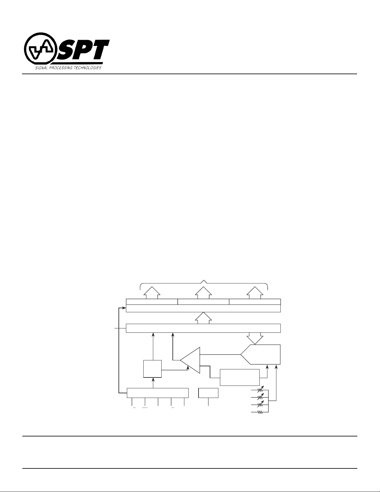
BLOCK DIAGRAM
Signal Processing Technologies, Inc.
Phone: (719) 528-2300 FAX: (719) 528-2370 Website: http://www.spt.com E-Mail: sales@spt.com
Output
Nibble A Nibble B Nibble C
Three-State Buffers And Control
STS
Clock
Control Logic
A
12/8 CS R/C
oCE
12-Bit SAR
Comp
+
-
Ref Out
Ref
Capacitance
Offset/Gain
Trim
20 V In
10 V In
BIP Off
AGND
4755 Forge Road, Colorado Springs, Colorado 80907, USA
12-Bit
DAC

ABSOLUTE MAXIMUM RATINGS (Beyond which damage may occur) 1 25 °C
Supply Voltages
Mode Control Voltage (VEE to DGND) ....................0 to +7 V
Logic Supply Voltage (VDD to DGND) ...................0 to +7 V
Analog to Digital Ground (AGND to DGND) .................±1 V
Input Voltages
Control Input Voltages (to DGND)
(CE, CS, Ao, 12/8, R/C)......................... -0.5 to VDD +0.5 V
Analog Input Voltage (to AGND)
(REF IN, BIP OFF, 10 VIN) ......................................±16.5 V
20 V VIN Input Voltage (to AGND) ..............................±24 V
Note: Operation at any Absolute Maximum Rating is not implied. See Operating Conditions for proper nominal applied
conditions in typical applications.
Output
Reference Output Voltage ..............Indefinite Short to GND
Momentary Short to V
Temperature
Operating Temperature, Ambient .................... 0 to +70 °C
Junction.........................+165 °C
Lead Temperature, (Soldering 10 Seconds)...........+300 °C
Storage Temperature....................................-65 to +150 °C
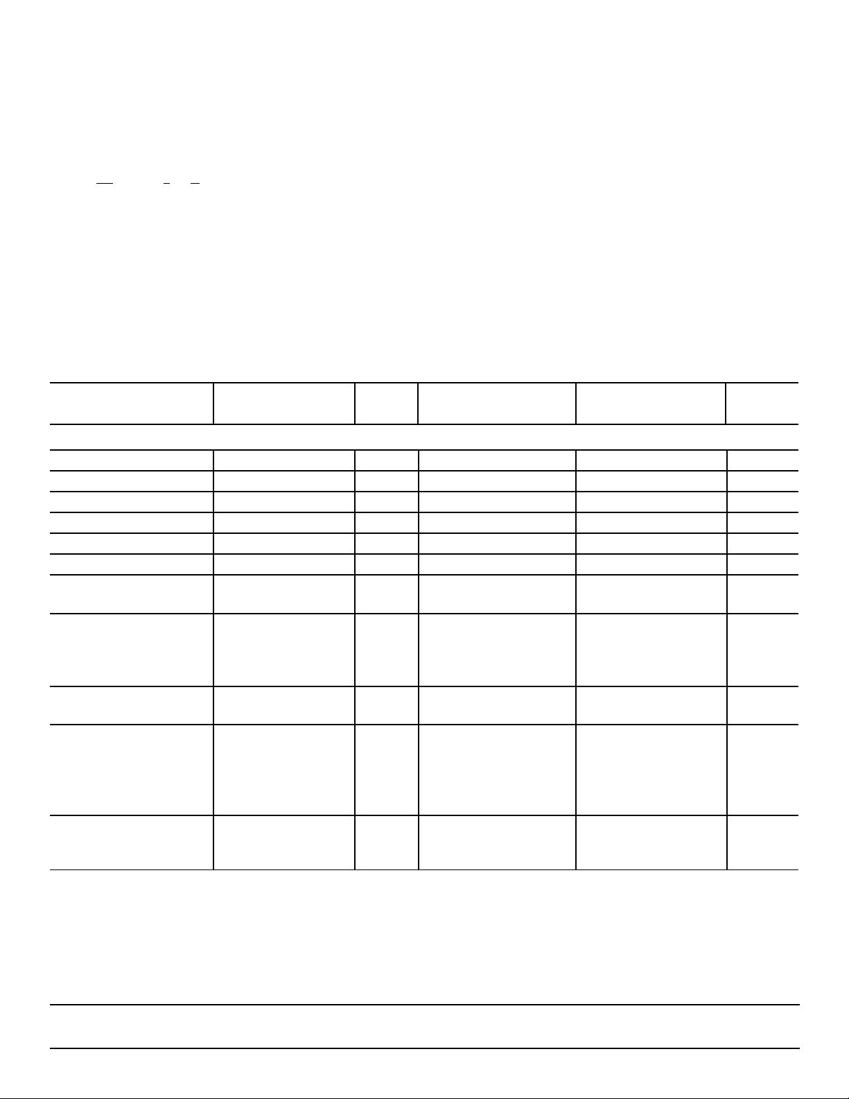
ELECTRICAL SPECIFICATIONS
DD
TA = T
PARAMETER CONDITIONS LEVEL MIN TYP MAX MIN TYP MAX UNITS
MIN
to T
MAX
, V
EE
= 0 to +5 V, V
TEST TEST SPT774C SPT774B
= +5 V, fS = 117 kHz, fIN = 10 kHz, unless otherwise specified..
DD
DC ELECTRICAL CHARACTERISTICS
Resolution VI 12 12 Bits
Linearity Error TA= 0 to +70 °CVI ±1 ±0.5 LSB
Differential Linearity No Missing Codes VI 12 12 Bits
Unipolar Offset; 10 V, 20 V +25 °C Adjustable to Zero VI ±2 ±2 LSB
Bipolar Offset; ±5 V, ±10 V +25 °C Adjustable to Zero VI ±10 ±4 LSB
Full Scale Calibration Error
Full Scale Calibration Error1No Adjustment to Zero
Temperature Coefficients Using Internal Reference
Unipolar Offset V ±1.0 ±1.0 ppm/°C
Bipolar Offset V ±2.0 ±2.0 ppm/°C
Full Scale Calibration V ±12 ±12 ppm/°C
Power Supply Rejection Max change in full VI ±0.5 ±0.5 LSB
+4.75 V<VDD<+5.25 V scale calibration
Analog Input Ranges
Bipolar VI -5 +5 -5 +5 Volts
Unipolar VI 0 +10 0 +10 Volts
Input Impedance
10 Volt Span VI 8.5 12 8.5 12 kΩ
20 Volt Span VI 35 50 35 50 kΩ
1
+25 °C Adjustable to Zero VI 0.30 0.30 % of FS
TA = 0 to +70 °C V 0.47 0.37 % of FS
VI -10 +10 -10 +10 Volts
VI 0 +20 0 +20 Volts
SPT
SPT774
2 8/1/00

ELECTRICAL SPECIFICATIONS
TA = T
MIN
to T
MAX
, V
EE
= 0 to +5 V, V
= +5 V, fS = 117 kHz, fIN = 10 kHz, unless otherwise specified.
DD
TEST TEST SPT774C SPT774B
PARAMETER CONDITIONS LEVEL MIN TYP MAX MIN TYP MAX UNITS
DC ELECTRICAL CHARACTERISTICS
Power Supplies Operating
Voltage Range
V
DD
2
V
EE
Operating Current
I
DD
IEE2V
= +5 V IV 167 167 µA
EE
Power Dissipation VI 75 120 75 120 mW
Internal Reference
Voltage VI 2.4 2.5 2.6 2.4 2.5 2.6 Volts
Output Current
3
DIGITAL CHARACTERISTICS
Logic Inputs
(CE,
, R/C, Ao, 12/8)
CS
Logic 0 VI -0.5 +0.8 -0.5 +0.8 Volts
Logic1 VI 2.0 5.5 2.0 5.5 Volts
Current VI -5.0 0. 1 5.0 -5.0 0. 1 5.0 µA
Capacitance V 5 5 pF
Logic Outputs
(DB11-DB0, STS)
Logic 0 (I
Logic 1 (I
= 1.6 mA) VI +0.4 +0.4 Volts
Sink
SOURCE
= 500 µA) VI +2.4 +2.4 Volts
Leakage (High Z State, VI -5 0.1 +5 -5 0.1 +5 µA
DB11-DB0 Only)
Capacitance V 5 5 pF
AC Accuracy fS=117 kHz, fIN=10 kHz
Spurious Free Dyn. Range V 73 78 76 78 dB
Total Harmonic Distortion V -77 -72 -77 -75 dB
Signal-to-Noise Ratio V 69 72 71 72 dB
Signal-to-Noise & Distortion V 68 71 70 71 dB
(SINAD)
Intermodulation Distortion fIN=20 kHz; V -75 -75 dB
f
=23 kHz
IN2
Note 1: Fixed 50 Ω resistor from REF OUT to REF IN and REF OUT to BIP OFF.
Note 2: VEE is optional and is only used to set the mode for the internal sample/hold. When not using VEE, the pin should be treated
as a no connect. If V
is connected to 0 to -15 V, aperture delay (tAP) will increase from 20 ns (typ) to 4000 ns (typ).
EE
Note 3: Available for external loads; external load should not change during conversion.
IV +4.5 +5.5 +4.5 +5.5 Volts
IV V
DD
V
DD
Volts
IV 15 24 15 24 mA
VI 0.5 0.5 mA
SPT
SPT774
3 8/1/00

ELECTRICAL SPECIFICATIONS
TA = T
MIN
to T
MAX
, V
EE
= 0 to +5 V, V
= +5 V, fS = 117 kHz, fIN = 10 kHz, unless otherwise specified.
DD
TEST TEST SPT774C SPT774B
PARAMETER CONDITIONS LEVEL MIN TYP MAX MIN TYP MAX UNITS
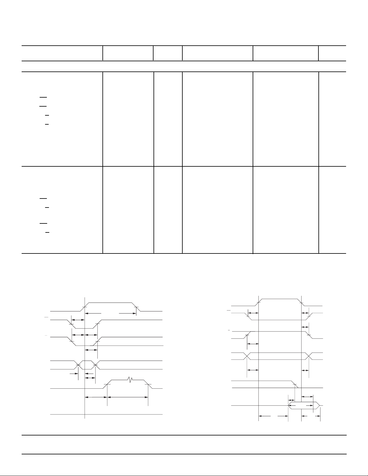
AC ELECTRICAL CHARACTERISTICS
4
Convert Mode Timing
t
STS Delay from CE VI 60 200 60 200 ns
DSC
t
CE Pulse Width VI 50 30 50 30 ns
HEC
t
CS to CE Setup VI 50 20 50 20 ns
SSC
CS Low during CE High VI 50 20 50 20 ns
t
HSC
R/C to CE Setup VI 50 0 50 0 ns
t
SRC
R/C Low During CE High VI 50 20 50 20 ns
t
HRC
t
Ao to CE Setup VI 0 0 ns
SAC
Ao Valid During CE High VI 50 20 50 20 ns
t
HAC
t
Conversion Time
C
5
12-Bit Cycle VI 7.5 8 7.5 8 µs
8-Bit Cycle VI 5.5 5.9 5.5 5.9 µs
Read Mode Timing
Access Time from CE VI 75 150 75 150 ns
t
DD
t
Data Valid After CE Low VI 25 35 25 35 ns
HD
t
Output Float Delay VI 100 150 100 150 ns
HL
CS to CE Setup VI 50 0 50 0 ns
t
SSR
R/C to CE Setup VI 0 0 ns
t
SRR
t
Ao to CE Setup VI 50 25 50 25 ns
SAR
CS Valid After CE Low VI 0 0 ns
t
HSR
R/C High After CE Low VI 0 0 ns
t
HRR
t
STS Delay After Data Valid VI 75 150 375 75 150 375 ns
HS
t
Ao Valid after CE Low VI 50 50 ns
HAR
Note 4: Time is measured from 50% level of digital transitions.
Note 5: Includes acquisition time.
Figure 1 - Convert Mode Timing Diagram Figure 2 - Read Mode Timing Diagram
CE
CE
CS
R/C
Ao
STS
DB11-DB0
SPT
t
t
t
SSC
SRC
SAC
t
t
t
t
DSC
High Impedance
HSC
HRC
HAC
t
HEC
t
C
4 8/1/00
R/C
STS
DB11-DB0
CS
Ao
t
SSR
t
SRR
t
SAR
HIGH
IMPEDANCE
t
DD
t
HSR
t
HRR
t
HAR
t
HS
DATA
VALID
t
HL
t
HD
SPT774
 Loading...